Jul 23, 2019

#IBM gives #cancer_killing drug AI project to the #OpenSource community | ZDNet https://t.co/GdgoUmx5UT https://t.co/lfC2v7MuFP


from Twitter https://twitter.com/wladek60

July 23, 2019 at 11:34AM
via IFTTT

CODEOCEAN: Charge-Based Modeling of Long-Channel Symmetric Double-Gate Junction FETs

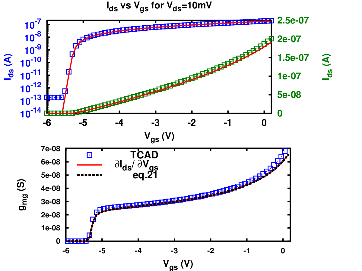
CODEOCEAN capsule written in OCTAVE which calculates the current and transconductances (gm, gmd and gms) using the charge based approach introduced in [1]. The capsule generates graphs demonstrating model versus TCAD simulations. The user can use the capsule code to experiment and reproduce the results in the paper [1]. 
The capsule is provided at the IEEE explorer site under the "Code&Datasets" link. https://ieeexplore.ieee.org/document/8371530 / doi: 10.1109/TED.2018.2838101 
Or at the link below https://codeocean.com/capsule/8244803/tree"

FIG: IdVg and gmVg at Vd=10mV
REF:
[1] N. Makris, F. Jazaeri, J. Sallese, R. K. Sharma and M. Bucher, "Charge-Based Modeling of Long-Channel Symmetric Double-Gate Junction FETs—Part I: Drain Current and Transconductances," in IEEE Transactions on Electron Devices, vol. 65, no. 7, pp. 2744-2750, July 2018.
doi: 10.1109/TED.2018.2838101
Abstract: The double-gate (DG) junction field-effect transistor (JFET) is a classical electron device, with a simple structure that presents many advantages in terms of not only device fabrication but also its operation. The device has been largely used in low-noise applications, but also more recently, in power electronics. Physics-based compact models for JFETs, contrary to MOSFETs, are, however, scarce. In this paper, an analytical, charge-based model is established for the mobile charges, drain current, and transconductances of symmetric DG JFETs, covering all regions of device operation. The model is unified and continuous from subthreshold to linear and saturation operation and is valid over a large temperature range. This charge-based model constitutes the basis of a full compact model of the DG JFET.
Keywords: junction gate field effect transistors;semiconductor device models;mobile charges;double-gate junction field-effect transistor;classical electron device;low-noise applications;power electronics;long-channel symmetric double-gate junction FET;symmetric DG JFET;charge-based modeling;physics-based compact models;drain current;Electric potential;JFETs;Logic gates;Integrated circuit modeling;Junctions;Mathematical model;MOSFET;Analytical model;circuit simulation;compact model;junction field-effect transistor (JFET);temperature effect


[paper] A Surface-Potential-Based Analytical I-V Model of Full-Depletion Single-Gate SOI MOSFETs

1
Department of Electrical and Electronic Teaching, 
College of Information Science and Engineering, 
Huaqiao University, Xiamen 361021, China

2
Department of Electronic Engineering, Jinan University, Guangzhou 510632, China
*
Correspondence: yufei_jnu@126.com; Tel.: +86-0592-6162-385
These two authors contributed equally to this work.

Received: 10 May 2019 / Accepted: 12 June 2019 / Published: 14 July 2019
Electronics 20198(7), 785; https://doi.org/10.3390/electronics8070785

Abstract

: 
A surface-potential-based analytical I-V model of single-gate (SG) silicon-on-insulator (SOI) MOSFETs in full-depletion (FD) mode is proposed and compared with numerical data and Khandelwal’s experimental results. An explicit calculation scheme of surface potential, processing high computation accuracy and efficiency, is demonstrated according to the derivation of the coupling relation between surface potential and back-channel potential. The maximum absolute error decreases into 10−7 V scale, and computation efficiency is improved substantially compared with numerical iteration. Depending on the surface potential, the drain current is derived in closed-form and validated by Khandelwal’s experimental data. High computation accuracy and efficiency suggest that this analytical I-V model displays great promise for SOI device optimizations and circuit simulations.

Keywords:
 silicon-on-insulator MOSFETs; surface potential; back-channel potential; full-depletion; analytical I-V model
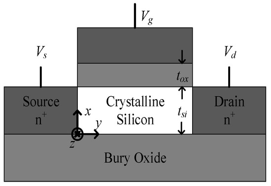
Figure 1. x-y cross section of silicon-on-insulator (SOI) MOSFETs.

Jul 12, 2019

IEEE ICECS 2019 paper submission deadline

ICECS 2019 paper deadline submission is approaching fast: July 15th, 2019

Please distribute this reminder to possible contributors and interested researchers and colleagues. Topics of interest include but are not limited to:

• Analog/mixed-signal/RF circuits
• Biomedical and Bio-Inspired Circuits and Systems
• EDA, Test and Reliability
• Digital circuits and systems
• Linear and Non-linear Circuits
• Low-Power Low-Voltage Design
• Microsystems
• Neural networks, Machine and Deep Learning
• Sensors and Sensing Systems
• Signal Processing, Image and Video
• VLSI Systems and Applications

The technical committee invites authors to submit 4-page papers in standard IEEE double-column format, including references, figures and tables, to clearly present the work, methods, originality, significance and applications of the techniques discussed.

Maurizio Valle; IEEE ICECS 2019 General Chair
https://www.ieee-icecs2019.org/