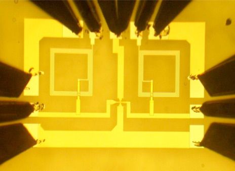
IBM researchers have built the first IC based on a graphene transistor. It is another step toward overcoming the limits of silicon and a potential path to flexible electronics [read more at spectrum.ieee.org]

Emerging technology and a developing infrastructure for printed electronics is enabling circuitry that is flexible, conformable, and inexpensive to mass-produce. FlexTech Alliance has identified, funded, and directed advanced development in the flexible and printed electronics infrastructure, paving the way for the practical manufacture of a variety of low-cost applications such as electronic packaging, ID tags, and wide-area lighting panels.
Printed electronics include a set of consumer markets where printed logic and memory will be required. The size and cost of fully printed systems is set to challenge silicon-based technologies in ultra-high-volume distributed applications. To address this issue, Norwegian firm ThinFilm Electronics produces rewritable memory tags manufactured using full roll-to-roll (R2R) printing. Printed non-volatile RAM (NVRAM), when combined with printed transistor elements, serves as the basis of a new generation of cheap, disposable, and highly ubiquitous electronic devices. The company is working with major toy and game companies and has established high-volume manufacturing to deliver millions of tags per month.
In other commercial development, a new method for fabricating printed semiconductors, developed by NthDegree Technologies, allows a standard high-speed printing press to print conductive ink on to paper, plastic, or other substrate materials. Printed semiconductors made with these inks reduce the cost of producing semiconductor-based devices while creating innovative conformable products. Wide-area lighting is currently being produced with this technology by means of a light-emitting diode (LED) "ink". This LED ink is being used to print area lighting that is converted into a flat panel to replace fluorescent tube fixtures.
These latest developments in printed electronics materials, tools and processes, including LED lighting and printed memory, will be discussed and demonstrated at the Extreme Electronics TechXpot session "Printed electronics: Beyond R&D to real-deal technologies," presented by the FlexTech Alliance at SEMICON West, July 14, 2011. For more information about FlexTech Alliance visit www.flextech.org.

Lisa Su, VP and general manager of Freescale"Some 7 billion devices will be connected to the Internet in this era from 2006 to 2020," said Lisa Su, vice president and general manager of Freescale Semiconductor Inc's networking and multimedia group. "And mobile traffic is doubling every year through 2015."
IEDM Abstract Submission Site is Now Open - Abstract Submission
Deadline:   June 24, 2011

2011 IEEE International Electron Devices Meeting
The Annual Technical Meeting of the Electron Devices Society will be held at the
Washington Hilton, Washington, DC USA  - December 5-7, 2011

To view the IEDM Call for Papers and instructions for submitting an abstract to
the conference, visit:      http://www.ieee-iedm.org

IEEE International Electron Devices Meeting (IEDM) is the world’s pre-eminent
forum for reporting technological breakthroughs in the areas of semiconductor
and electronic device technology, design, manufacturing, physics, and modeling.
IEDM is the flagship conference for nanometer-scale CMOS transistor technology,
advanced memory, displays, sensors, MEMS devices, novel quantum and nano-scale
devices and phenomenology, optoelectronics, devices for power and energy
harvesting, high-speed devices, as well as process technology and device
modeling and simulation.

Starting this year (2011) there is an increased emphasis on circuit and device
interaction.  With ever increasing transistor count, nanometer design rules and
layout restrictions, circuit-device interaction is becoming critical to
providing viable technology solutions. This new emphasis includes
technology/circuit co-optimization, power/performance/area analyses, design for
manufacturing and process control, as well as CMOS platform technology and
scaling.

INCREASED PARTICIPATION IN THE FOLLOWING AREAS IS SOUGHT:
 * Circuit-device interaction
 * Energy harvesting
 * Biomedical devices
 * Power devices

Information about IEDM can be found at: http://www.ieee-iedm.org
Twitter: http://twitter.com/ieee_iedm
Facebook: http://www.facebook.com/pages/IEDM/131119756449

MEETING HIGHLIGHTS
 * New subcommittees (Circuit-Device Interaction and Nano Device Technology)
 * New for 2011:  90 Minute Tutorial Sessions on Emerging Topics, Saturday
afternoon, December 3
 * Three plenary presentations by prominent experts
 * Invited papers on all aspects of advanced devices and technologies.
 * An Emerging Technology session.
 * Two evening Panel discussions.
 * Presentation of IEEE/EDS awards.
 * IEDM Luncheon presentation will be held on Tuesday, December 6.
 * Two short courses will be held on Sunday, December 4.

Further Information - All questions or inquiries for further information
regarding this meeting should be directed to the Conference Office at:

19803 Laurel Valley Place
Montgomery Village, MD 20886 USA
Tel: 301-527-0900, ext. 2
Email: iedm@his.com
Local European Contact

Stefan De Gendt, IMEC, Belgium
Local Asian Contact
Norikatsu Takaura, LEAP, Japan
2011 Conference Chair
Kazunari Ishimaru, Toshiba, Japan
Technical Program Chair
Veena Misra, North Carolina State University, USA

If you know of any colleagues who may have a paper to contribute and have not
received this notice, please bring it to their attention.