Dec 22, 2020

[paper] Radiation testing of a 6-axis MEMS inertial navigation unit

Radiation testing of a commercial 6-axis MEMS inertial navigation unit at ENEA Frascati proton linear accelerator
G. Bazzanoa,b, A. Ampollinia, F. Cardellia, F. Fortinia, P. Nenzia, G.B. Palmerinib, L. Picardia
L. Piersantia, C. Ronsivallea, V. Surrentia, E. Trincaa, M. Vadruccia, M. Sabatinic
Advances in Space Research (2020)
DOI: 10.1016/j.asr.2020.11.031
aENEA, Via Enrico Fermi 45, Frascati, Italy
bScuola di Ingegneria Aerospaziale, La Sapienza Università di Roma, Italy
cDipartimento di Ingegneria Astronautica, Elettrica ed Energetica, La Sapienza Università di Roma, Italy 

Abstract: We present the first results of a novel collaboration activity between ENEA Frascati Particle Accelerator Laboratory and University La Sapienza Guidance and Navigation Laboratory in the field of Radiation Hardness Assurance (RHA) for space applications. The aim of this research is twofold: (a) demonstrating the possibility to use the TOP-IMPLART proton accelerator for radiation hardness assurance testing, developing ad hoc dosimetric and operational procedures for RHA irradiations; (b) investigating system level radiation testing strategies for Commercial Off The Shelf (COTS) components of interest for SmallSats space missions, with focus on devices and sensors of interest for guidance, navigation and control, through simultaneous exploration of Total Ionizing Dose (TID), Displacement Damage (DD) dose and Single-Event Effects (SEE) with proton beams. A commercial 6-axis integrated Micro Electro-Mechanical Systems (MEMS) inertial navigation system (accelerometer, gyroscope) was selected as first Device Under Test (DUT). The results of experimental tests aimed to define an operational procedure and the characterization of radiation effects on the component are reported, highlighting the consequence of the device performance degradation in terms of the overall navigation system accuracy. Doses up to 50 krad(Si) were probed and cross sections for Single-Event Functional Interrupt (SEFI) evaluated at a proton energy of 30 MeV. 
Fig: Polyedric support for MEMS accelerometer characterization


Dec 21, 2020

[paper] Cross Domain Modeling of a Meander Beam MEMS Accelerometer

Mahdieh Shojaei Baghini*

*Department of Mechanical, Maritime and Materials Engineering, Delft University of Technology, Delft, Netherlands

Abstract: This paper presents the design of a bulk Silicon MEMS single-axis 8-beam accelerometer utilizing meander beams in the Structural Mechanics and MEMS Module of COMSOL Multiphysics®. To obtain further insights into the design of the accelerometer, an electrical lumped element model of the structure is derived and represented in SPICE. Quantities such as eigenfrequencies and proofmass displacement have been extracted from COMSOL Multiphysics® as well as analytical studies. The effects of parasitic frequencies in the structure are observed by automatic tilting of the accelerometer at higher order eigenfrequencies due to finite off-axis stiffness coefficients. In order to mathematically quantify the response of the accelerometer arising due to parasitic frequencies, the transient damping response has been derived in COMSOL Multiphysics® as well as SPICE, and the differences are highlighted. Finally, the eigenfrequencies of the meanderbeam accelerometer have been compared with that of a simple-beam accelerometer and the validity of small deflection theory is tested for the lumped model approach. While the target damping factor of the accelerometer was 0.7, the obtained damping factor increased to 1.1 due to the aforementioned parasitic frequencies and reduction in the resonance frequency of the sensor. This effect was precisely captured during the COMSOL Multiphysics® simulation.
Fig: The designated sensor is damped using plates placed at a distance equal to h0; its a) electrical circuit equivalent of squeeze-film damped accelerometer; b) electrical circuit considering symmetric damping; c) simplified equivalent circuit for gap height derivation.


Dec 15, 2020

[VIRTUAL] EDS MQ on Compact Modeling

VIRTUAL MINI-COLLOQUIUM ON COMPACT MODELING


IEEE EDS Compact Modeling Technical Committee
EDS Spain Chapter
Department of Electronic, Electrical and Automatic Control Engineering, 
University Rovira I Virgili, Tarragona (Spain)

December 17, 2020
EDS MQ Program (times in CET)
10:20-10:30
Benjamin Iñiguez, IEEE EDS MQ Chair
Department of Electronic, Electrical and Automatic Control Engineering, University Rovira I Virgili, Tarragona (Spain)
Opening session
10:30-11:15
Yogesh. S Chauhan
Department of Electrical Engineering,
Indian Institute of Technology Kanpur (India)
BSIM-BULK and BSIM-HV: Industry Standard SPICE Models for Analog, RFand High Voltage Applications
11:15-12:00
Manoj Saxena
Department of Electronics, University of Delhi  (India)
“Modeling and Simulation of Robust Ultrasensitive Tunnel Field Effect Transistor Design for Biosensing Applications”
12·00-12:45
Wladek Grabinski
GMC, Commugny (Switzerland)
FOSS TCAD/EDA Tools for Semiconductor Device Modeling
12:45-13:30
Arokia Nathan
Darwin College, University of Cambridge (UK)
“Physics-Based Parameter Extraction for TFTs”
13:30-15:00 Break
15:00-15:45
Marcelo Pavanello
Department of Electrical Engineering,
Centro Universitario FEI, Sao Bernardo do Campo (Brazil)
"Quantum Effects on the Mobility of SOI Nanowire MOSFETs Induced by the Active Substrate Bias"
15:45-16:30
Michael S. Shur
Department of Electrical, Systems and Computer Engineering,
Rensselaer Polytechnic Institute, Troy NY (USA)
THz Compact SPICE/ADS model
16:30-17:15
Edmundo Gutiérrez
Department of Electronics, INAOE, Puebla (Mexico)
"RF MOSFET degradation modeling up to 67 GHz”
End of EDS MQ

Dec 12, 2020

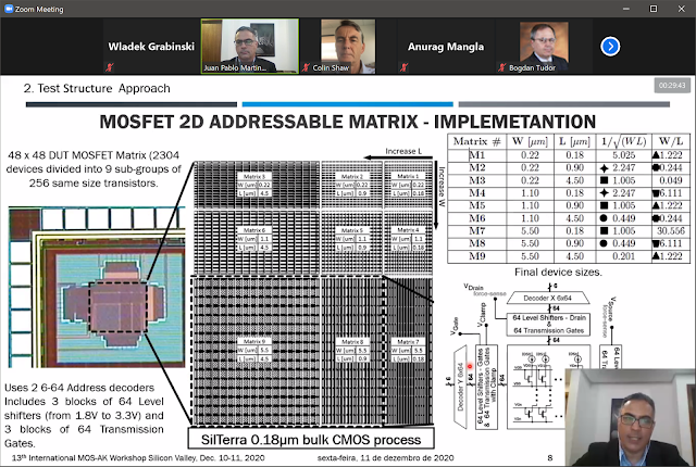
[2nd Day Photos] 13th International MOS-AK Workshop

13th International MOS-AK Workshop was organized jointly with THM Giessen who has provided ZOOM meeting platform for the online event. 50+ registered participants have attended 2nd day with two further MOS-AK sessions and followed 7 technical talks

MOS-AK session III - 11:00 - 14:00 (PST) on Dec.11, 2020
Chair: Anurag Mangla; Semtech Neuchatel (CH)

[8] Statistical Analysis of MOSFET extracted parameters for n-MOS mismatch modeling.
Juan Pablo Martinez Brito
CEITEC SA/UFRGS (BR)

[9] Rapid multiscale simulation of nanoscale MOSFETs: Is an interplay between compact models and NEGF possible?
Alexander Kloes
NanoP, THM University of Applied Sciences (D)


[10] The Effect of Non Rectangular MOS Channels in Modelling High Voltage Lateral MOS
Marco Sambi, Lorenzo Labate, Simona Cozzi, Nicola Holzer
STMicroelectronics (I)

MOS-AK session IV
Chair: Daniel Tomaszewski, Lukasiewicz - IMiF, Warsaw (PL)

[11] Nonlinear Embedding Model for the Accelerated Design of PAs with the ASM-HEMT model
Patrick Roblin*, Miles Lindquist*, Nicholas Miller+ and Marek Mierzwinski^
*The Ohio State University, AFRL+, Keysight Corp.^ (USA)

[12] New analytical model for AOSTFTs
Antonio Cerdeira, Yoanlys Hernandez-Barrios, Magali Estrada, Benjamin Iniguez
CINVESTAV (MX) and URV (SP)

[13] Unifying the Modeling of Charge Trapping in RTN, 1/f Noise and BTI
Gilson Wirth
UFRGS (BR)

[14] SPICE Modeling for Display Technologies
Bogdan Tudor
Silvaco (USA)

MOS-AK attendees group photo of 2nd MOS-AK workshop day:

MOS-AK attendees group photo (1)

MOS-AK attendees group photo (2)


Dec 11, 2020

[1st Day Photos] 13th International MOS-AK Workshop


13th International MOS-AK Workshop was organized jointly with THM Giessen who has provided ZOOM meeting platform for the online event. More than 50 registered participants have attended two MOS-AK sessions and followed 7 technical talk during its first day.

MOS-AK session I - 11:00 - 14:00 (PST) on Dec.10, 2020
Chair: Laurie E. Calvet; CNRS-University Paris-Saclay (F)

[1] Material Growth, Characterization of III-V & II-VI Compound Semiconductors and its Use for Various Device Applications
Saxena Praveen Kumar
Tech Next Lab Pvt Ltd (IN)

[2] Contact-controlled transistors: Device characteristics and modelling challenges
Radu Sporea
Uni. Surrey (UK)

[3] Contact-controlled transistors: Specific applications and opportunities
Eva Bestelink
Uni. Surrey (UK)

MOS-AK session II
Chair: Larry Nagel; Omega Enterprises Consulting (USA)

[4] 90 Years of Twoport Matrices and its Impact on Device Measurements and Modeling
Franz Sischka
SisConsult Engineering Office (D)

[5] Some issues on the high-frequency compact modeling of CMOS transistors and related devices
Roberto Murphy
INAOE (MX)

[6] VAMPyRE: Verilog-A Model Pythonic Rule Enforcer
Geoffrey Coram
Analog Devices, Inc. (USA)

[7] Simulate 40X Faster with SmartSpice HPP
Jody Matos
Silvaco (USA)

MOS-AK attendees group photo of 1st MOS-AK workshop day:

MOS-AK attendees group photo (1)

MOS-AK attendees group photo (2)