Departament d’Enginyeria Electrònica, Escola d’Enginyeria, Universitat Autònoma de Barcelona, Bellaterra 08193 (SP)
Departamento de Electrónica y Tecnología de Computadores, Universidad de Granada, 18011 Granada (SP)
| Capability | Existing State-of-the-Art | Proposed AI/ML Approach | Best Prior AI/ML Approach |
|---|---|---|---|
| obeys the laws of thermodynamics | ✓ | ? | ? |
| accurate DC modeling for all terminal currents, on relevant log/linear scale | ✓ | ? | ? |
| accurate capacitance/charge modeling | ✓ | ? | ? |
| models DC and capacitance interaction where relevant | ✓ | ? | ? |
| accurate modeling of high-frequency/non-quasi-static effects where relevant | ✓ | ? | ? |
| works for large-signal transient simulation, including delay effects | ✓ | ? | ? |
| accurate noise modeling | ✓ | ? | ? |
| has full geometry dependence | ✓ | ? | ? |
| has complete temperature dependence | ✓ | ? | ? |
| models all necessary LDEs | ✓ | ? | ? |
| behaves “well” for unreasonable geometry or temperature or bias | ✓ | ? | ? |
| exhibits physical monotonicity over bias, geometry, and temperature | ✓ | ? | ? |
| is smooth (ideally C∞-continuous) | ✓ | ? | ? |
| exhibits relevant physical symmetries (currents, charges, their derivatives) | ✓ | ? | ? |
| exhibits asymptotic correctness over geometry, temperature, and bias | ✓ | ? | ? |
| includes modeling of electrothermal effects (with frequency dependence) | ✓ | ? | ? |
| includes, or enables, modeling of global and local statistical variation | ✓ | ? | ? |
| includes, or enables, modeling of aging | ✓ | ? | ? |
| enables modeling of parasitics for different layouts | ✓ | ? | ? |
| is verified to converge reliably in at least one circuit simulator | ✓ | ? | ? |
| IMPORTANT DATES
Abstract Submission Deadline January 15, 2025 Acceptance Notifications March 10, 2025 Full Paper Submission Deadline April 20, 2025 ORGANIZING COMMITTEE General Chair Peter M. Lee Micron Vice Chair Shahed Reza Sandia Lab Technical Program Chair Colin Shaw Silvaco Technical Program Vice Chair Gert-Jan Smit NXP Treasurer Leigh Anne Clevenger Si2 Secretariat Conference Catalysts icmc@conferencecatalysts.com ![]() |
The Compact Model Coalition (CMC) brings academia and industry partners together in the development and standardization of compact models for semiconductor devices. For 30 years now, the CMC has been instrumental in creating standardized and verified models for designers to use in their increasingly complex circuits for SPICE simulation. The CMC is organizing a new and innovative International Compact Modeling Conference. Cosponsored by IEEE EDS, it will focus uniquely on compact device models, their development and broad application in the semiconductor industry. You are invited to participate in the evolution of these models, guide model development to help circuit designers create the best circuit performance possible, and enable foundries to leverage the strength of their device fabrication to full extent. Join the world experts in design, process technology, and model development to discuss state-of-the-art semiconductor device modeling for a two-day in-person event in one location, offering a great opportunity to present and learn about this core element of circuit design and how to get the most from these global collaborations. We are seeking papers for oral or poster presentations in the following areas: APPLICATION OF DEVICE MODELS
Please submit your paper proposals in the form of a 2-page abstract for review by
January 15, 2025 here 2025.si2-icmc.org. Acceptance notifications will be sent by
March 10, 2025. Accepted contributions (for both oral and poster presentations) are
expected to submit a camera-ready 4-page draft version of their papers by April 20,
2025 and final version by May 23, 2025 for publication in IEEE Xplore®. |
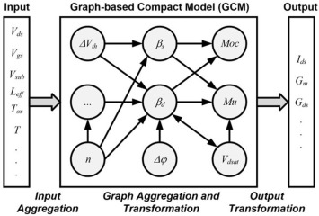
Abstract: Neural compact models are proposed to simplify device-modeling processes without requiring domain expertise. However, the existing models have certain limitations. Specifically, some models are not parameterized, while others compromise accuracy and speed, which limits their usefulness in multi-device applications and reduces the quality of circuit simulations. To address these drawbacks, a neural compact modeling framework with a flexible selection of technology-based model parameters using a two-stage neural network (NN) architecture is proposed. The proposed neural compact model comprises two NN components: one utilizes model parameters to program the other, which can then describe the current–voltage (IV) characteristics of the device. Unlike previous neural compact models, this two-stage network structure enables high accuracy and fast simulation program with integrated circuit emphasis (SPICE) simulation without any trade-off. The IV characteristics of 1000 amorphous indium–gallium–zinc-oxide thin-film transistor devices with different properties obtained through fully calibrated technology computer-aided design simulations are utilized to train and test the model and a highly precise neural compact model with an average IDS error of 0.27% and R2 DC characteristic values above 0.995 is acquired. Moreover, the proposed framework outperforms the previous neural compact modeling methods in terms of SPICE simulation speed, training speed, and accuracy.
Chapter: Differential Equation-Based Compact 2-D Modeling of Asymmetric Gate Oxide Heterojunction Tunnel FET; By: Sudipta Ghosh, Arghyadeep Sarkar
Abstract: Tunnel Field Effect Transistor (TFET) has emerged as an effective alternative device to replace MOSFET for a few decades. The major drawbacks of MOSFET devices are the short-channel effects, due to which the leakage current increases with a decrease in device dimension. So, scaling down TFET is more efficacious than that of MOSFETs. Sub-threshold swing (SS) is another advantageous characteristic of TFET devices for high-speed digital applications. In TFETs the SS could be well below 60 mV/decade, which is the thermal limit for MOSFET devices and therefore makes it more suitable than MOSFET for faster switching applications. It is observed from the literature studies that the performances of the TFET devices have been explored thoroughly by using 2-D TCAD simulation but an analytical model is always essential to understand the physical behavior of the device and the physics behind this; which facilitates further, the analysis of the device performances at circuit level as and when implemented.
|
![]() |
|
| Organized
by:
University of Udine (Italy) Conference chair: Pierpaolo Palestri Local organizing Committee: Francesco Driussi Conference Secretariat: Centro Congressi Internazionali Steering Committee:
|
8th Joint
International EuroSOI Workshop and International Conference on Ultimate Integration on Silicon (EuroSOI-ULIS) 2022 May 18-20, 2022 – Udine, Italy https://eurosoiulis2022.com The Conference aims at gathering
together scientists and engineers working in academia, research centers
and industry in the field of SOI technology and nanoscale devices in
More-Moore and More-Than-Moore scenarios. High quality contributions in the following areas are
solicited:
Original 2-page abstracts with
illustrations will be reviewed by the Scientific Committee. The
accepted contributions will be published as 4-page letters in a special
issue of the Elsevier journal Solid-State Electronics.
Extended versions of outstanding papers will be published in a further
special issue of Solid-State Electronics. A best poster award will be
attributed by ELSEVIER.
The “Androula
Nassiopoulou Best Paper Award" will be attributed by the
SINANO institute.
Important dates:
|
Abstract: Memristors are among the most promising devices for building neural processors and non-volatile memory. One circuit design stage involves modeling, which includes the option of memristor models. The most common approach is the use of compact models, the accuracy of which is often determined by the accuracy of their parameter extraction from experiment results. In this paper, a review of existing extraction methods was performed and new parameter extraction algorithms for an adaptive compact model were proposed. The effectiveness of the developed methods was confirmed for the volt-ampere characteristic of a memristor with a vertical structure: TiN/HfxAl1-xOy/HfO2/TiN.
[1] N. Chatterjee, J. Ortega, I. Meric, P. Xiao and I. Tsameret, "Machine Learning On Transistor Aging Data: Test Time Reduction and Modeling for Novel Devices," 2021 IEEE International Reliability Physics Symposium (IRPS), 2021, pp. 1-9, doi: 10.1109/IRPS46558.2021.9405188.
Abstract: Accurately modeling the I-V characteristics and current degradation for transistors is central to predicting circuit end-of-life behavior. In this work, we propose a machine learning model to accurately model current degradation at various stress conditions and extend that to make nominal use-bias predictions. The model can be extended to track and predict any parametric change. We show an excellent agreement of the model with experimental results. Furthermore, we use a deep neural network to model the I-V characteristics of aged transistors over a wide drain and gate playback bias range and show an excellent agreement with experimental results. We show that the model is reliably able to interpolate and extrapolate demonstrating that it learns the underlying functional form of the data.
URL: https://ieeexplore.ieee.org/stamp/stamp.jsp?tp=&arnumber=9405188&isnumber=9405088
[2] P. B. Vyas et al., "Reliability-Conscious MOSFET Compact Modeling with Focus on the Defect-Screening Effect of Hot-Carrier Injection," 2021 IEEE International Reliability Physics Symposium (IRPS), 2021, pp. 1-4, doi: 10.1109/IRPS46558.2021.9405197.
Abstract: Accurate prediction of device aging plays a vital role in the circuit design of advanced-node CMOS technologies. In particular, hot-carrier induced aging is so complicated that its modeling is often significantly simplified, with focus limited to digital circuits. We present here a novel reliability-aware compact modeling method that can accurately capture the full post-stress I-V characteristics of the MOSFET, taking into account the impact of drain depletion region on induced defects.
URL: https://ieeexplore.ieee.org/stamp/stamp.jsp?tp=&arnumber=9405197&isnumber=9405088
[3] Z. Wu et al., "Physics-based device aging modelling framework for accurate circuit reliability assessment," 2021 IEEE International Reliability Physics Symposium (IRPS), 2021, pp. 1-6, doi: 10.1109/IRPS46558.2021.9405106.
Abstract: An analytical device aging modelling framework, ranging from microscopic degradation physics up to the aged I-V characteristics, is demonstrated. We first expand our reliability oriented I-V compact model, now including temperature and body-bias effects; second, we propose an analytical solution for channel carrier profiling which-compared to our previous work-circumvents the need of TCAD aid; third, through Poisson's equation, we convert the extracted carrier density profile into channel lateral and oxide electric fields; fourth, we represent the device as an equivalent ballistic MOSFETs chain to enable channel “slicing” and propagate local degradation into the aged I-V characteristics, without requiring computationally-intensive self-consistent calculations. The local degradation in each channel “slice” is calculated with physics-based reliability models (2-state NMP, SVE/MVE). The demonstrated aging modelling framework is verified against TCAD and validated across a broad range of VG/VD/T stress conditions in a scaled finFET technology.
URL: https://ieeexplore.ieee.org/stamp/stamp.jsp?tp=&arnumber=9405106&isnumber=9405088