Jan 31, 2024

[paper] THz Measurements, Antennas, and Simulations

Fawad Sheikh 1, Andreas Prokscha 1, Johannes M. Eckhardt 2, Tobias Doeker 2, Naveed A. Abbasi 3, Jorge Gomez-Ponce 3,4, Benedikt Sievert 5, Jan Taro Svejda 5, Andreas Rennings 5, Jan Barowski 6, Christian Schulz 6, Ilona Rolfes 6, Daniel Erni 5, Andreas F. Molisch 3, Thomas Kürner 2, and Thomas Kaiser 1
THz Measurements, Antennas, and Simulations: From the Past to the Future
Invited Paper in IEEE Journal of Microwaves, vol. 3, no. 1, pp. 289-304, Jan. 2023
DOI: 10.1109/JMW.2022.3216210

1 Institute of Digital Signal Processing, UDE, Duisburg (D)
2 Institute for Communications Technology, TU Braunschweig (D)
3 Wireless Devices and Systems Group, University of Southern California, Los Angeles (USA) 
4 ESPOL, Facultad de Ingeniería en Electricidad y Computación, Guayaquil (EC)
5 ATE, University of Duisburg-Essen, and CENIDE Duisburg (D)
6 Institute of Microwave Systems, Ruhr University, Bochum (D)

Abstract: In recent years, terahertz (THz) systems have become an increasingly popular area of research thanks to their unique properties such as extremely high data rates towards Tb/s, submillimeter localization accuracy, high resolution remote sensing of materials, and remarkable advances in photonics and electronics technologies. This article traces the progress of the THz measurements, antennas and simulations, from historical milestones to the current state of research and provides an outlook on the remaining challenges.

FIG: Realized gain measurement of the integrated antenna prototype compared to the estimation of the corresponding equivalent circuit (EC) model in E- and H-plane at 290GHz (a)
and micrograph of the antenna prototype (b)

AcknowledgmentThis work was supported in part by Deutsche Forschungsgemeinschaft for Projects M01, M02, M03, M04, C05, and S03, under Project 287022738 TRR 196, in part by the Ministry of Culture and Science of the State of North Rhine-Westphalia (MKW NRW) through Project terahertz.NRW, and in part by the Open Access Publication Fund of the University of Duisburg-Essen. The work of Jorge Gomez-Ponce was supported by Foreign Fulbright Ecuador SENESCYT Program. The work of Johannes M. Eckhardt, Tobias Doeker, and Thomas Kürner was supported in part by the Federal Ministry of Education and Research (BMBF), Germany, through 6G Research and Innovation Cluster 6G-RIC under Grant 16KISK031 and in part by German Research Foundation (DFG) under Grant FOR 2863, “Meteracom - Metrology for THz Communications.” The work of Jorge Gomez-Ponce, Naveed A. Abbasi, and Andreas F. Molisch was supported by SRC, DARPA, NSF, NIST, and Samsung Research America through ComSenTer Program. This work did not involve human subjects nor animals in its research.


Jan 29, 2024

List of the publications using or referring to DEVSIM

List of the publications using or referring to DEVSIM
[1] K. Wang et al.; Design and simulation of a novel 4H-SiC LGAD timing device; Radiation detection technology and methods; (2023) https://doi.org/10.1007/s41605-023-00431-y
[2] J. Lauwaert; Technology computer aided design based deep level transient spectra: Simulation of high-purity germanium crystals; Journal of Physics D: Applied Physics; (2022) https://doi.org/10.1088/1361-6463/ac34ad
[3] Q. Chen et al.; Analytical model for donor like Gaussian traps in organic thin-film transistor; Organic Electronics; (2021) https://doi.org/10.1016/j.orgel.2022.106464
[4] Q. Chen et al.; The Impact of Contact Position on the Retention Performance in Thin-Film Ferroelectric Transistors; Physica Status Solidi A; (2021) https://doi.org/10.1002/pssa.202100408
[5] L. Hulbert; Designing a Simulator for an Electrically-Pumped Organic Laser Diode; Master’s Thesis; (2019) https://doi.org/10.15368/theses.2019.60
[6] J. E. Sanchez and Q. Chen; Element Edge Based Discretization for TCAD Device Simulation; IEEE Transactions on Electron Devices; (2021) https://doi.org/10.1109/TED.2021.3094776
[7] J. Lauwaert; Fill Factor Loss in a Recombination Junction for Monolithic Tandem Solar Cells; ACS Appl. Energy Mater.; (2023) https://doi.org/10.1021/acsaem.3c00041
[8] J. E. Sanchez; DEVSIM: A TCAD Semiconductor Device Simulator; Journal of Open Source Software; (2022) https://doi.org/10.21105/joss.03898
[9] L. Rickert et al.; High-performance designs for fiber-pigtailed quantum-light sources based on quantum dots in electrically-controlled circular Bragg gratings; Optics Express; (2023) https://doi.org/10.1364/OE.486060
[10] L. R. Brennaman & A. J. Samin; Insights into the performance of InAs-based devices in extreme environments from multiscale simulations; Applied Physics A; (2023) https://doi.org/10.1007/s00339-023-06756-1
[11] M. D. K Jones et al.; Modelling Interfaces in Thin-Film Photovoltaic Devices; Frontiers in Chemistry; (2022) https://doi.org/10.3389/fchem.2022.920676
[12] R. Sellers et al.; fabrication and modeling study to reduce valence band offset in HgCdTe MWIR nBn photodetectors grown on silicon using superlattice barriers; Proc. SPIE PC12687, Infrared Sensors, Devices, and Applications XIII,; (2023) https://doi.org/10.1117/12.2677394
[13] TANG Zhenglai and CAO Bingyang ; Simulations of self-heating effects and the heat generation mechanisms in SOI-MOS devices; Microelectronics & Computer; (2023) https://doi.org/10.19304/J.ISSN1000-7180.2023.0630
[14] Kotecha et al.; Modeling Needs for Power Semiconductor Devices and Power Electronics Systems; IEDM (2019) (2019) https://doi.org/10.1109/IEDM19573.2019.8993449

Postdoc in Semiconductor Devices, and circuit design


Postdoc in Semiconductor Devices, and circuit design
Sønderborg, Denmark

We [sdu.dk] are seeking an enthusiastic new colleague as a PostDoc in the field of Semiconductor Devices, and circuit design. As a postdoc in our team, you will have the opportunity to contribute to cutting-edge research and innovation in this rapidly evolving field with a strong collaboration with international industry partners.

The position is located in the section of Electrical Engineering in Sønderborg within the Centre for Industrial Electronics (CIE). The Centre has currently approximately 30 faculty members including senior (full and associate professors), junior (assistant professors and postdocs), PhDs, and support staff. The task portfolio of the PostDocs will be linked to one main project and several smaller projects within CIE. CIE is embedded in a powerhouse in electronics, which includes researchers and developers at universities and industries on both sides of the Danish-German border. CIE is a new initiative striving for high quality and great impact of its research, innovation, and education. Central to achieving this objective is access to state-of-the-art facilities and collaborations with industries. In the semiconductor research group in CIE, we are a member of European projects and already settled our international collaborations with the pioneer industry.

The positions aim to build strong knowledge and competencies within the field of semiconductor devices, especially in the fields of wide band gap semiconductor devices, circuit design, failure mechanisms, and simulations.

Job description
  • Conduct research in the field of WBG semiconductors with a focus on GaN and SiC devices.
  • Innovate design structures through simulation-based approaches calibrated by experimental data.
  • Apply TCAD simulation and design tools, build demonstrators, and verify your simulation by experimental measurements.
  • Familiar with the fabrication process to realize devices in the clean room and explore their potential applications.
  • Experimental characterization of devices (static and dynamic) to analyze the device behavior.
  • Stay updated with the latest advancements in WBG semiconductor devices and contribute to the development of innovative solutions.
  • You will be involved in the daily supervision of PhD, Master, and Bachelor students who perform research on similar topics.
  • You will publish and present your work both at international conferences and in scientific journals with high impact.
Profile and requirements 
  • Ph.D. in Electrical Engineering, Semiconductor Physics, or a related field.
  • Strong background in theory and simulation of WBG semiconductor devices, device modeling, and circuit design.
  • Hands-on experience in fabrication processes such as lithography, Mask design, etching, and deposition appreciated.
  • Background in characterization techniques, failure mechanisms, and reliability tests.
  • Ability to work independently as well as collaboratively in a research team.
  • Strong communication skills to effectively present research findings and contribute to scientific discussions.
  • Ability to publish in high-impact conferences and journals.
Starting date: March 2024.
Type of contract: Full-time
Employment: 2-year position

Further information is available from 
Professor Thomas Ebel, Head of CIE, phone: +45 93 50 72 05 
Associate Professor Samaneh Sharbati, phone: +45 65 50 82 60

Conditions of employment

Employment as a postdoc requires scientific qualifications at PhD level. Employment as a postdoc is temporary and will cease without further notice at the end of the period. The successful applicant will be employed in accordance with the agreement between the Ministry of Finance and the Danish Confederation of Professional Associations

The assessment process

Read about the Assessment and selection process. Shortlisting may be used.

Application procedure
  • The application must be in English and must include:Motivated application
  • Detailed Curriculum Vitae
  • Certificates/Diplomas (MSc and PhD)
  • List of publications, indicating the publications attached
  • Examples of the most relevant publications. Please attach one pdf-file for each publication
  • Reference letters and other relevant qualifications may also be included.

Formalities
Documents should not contain a CPR number (civil registration number) – in this case, the CPR number must be crossed out. The application and CV must not exceed 10 MB. If you experience technical problems, you must contact hcm-support@sdu.dk.

The application deadline is 20. February 2024 at 23.59.

Further information for international applicants about entering and working in Denmark.

Further information about The Faculty of Engineering.

The University of Southern Denmark wishes to reflect the surrounding community and therefore encourages everyone, regardless of personal background, to apply for the position.


Open PhD Position at THM

Open PhD Position
Compact Modeling of Reconfigurable Transistors
(full-time)
Payment depending on qualification up to salary group 13 TV-H
(approx. 60k€ … 65k€ per year)

The position in Prof. Dr. Alexander Kloes' Research Group Nanoelectronics/Device Modeling at Technische Hochschule Mittelhessen (THM), University of Applied Sciences, Campus Giessen, is expected to be filled from May 2024 for a duration of 3 years. It is intended to enable the successful candidate to obtain a doctorate degree in a cooperative doctorate procedure between the THM University of Applied Sciences and the Universitat Rovira i Virgili (URV, Spain).
The project in the research field of microelectronics aims at compact modelling of reconfigurable MOS transistors. The goal of the project is the development of a DC/AC Verilog-A compact model for standard design tools to be used for new circuit design concepts in the field of hardware security. Starting point is a physics-based analytical compact current model for Schottky Barrier Transistors which has already been published by the research group at THM. The task is part of a joint project with academic and industrial partners in areas from device technology to logic synthesis. Beside TCAD simulations, for verification by measurements, the project is in close collaboration with a global company for the fabrication of test structures.

Your Tasks:
  • Research in the field of microelectronics and physics of semiconductor devices
  • PhD project on the development of a compact model for reconfigurable MOSFETs
  • Implementation in standard design tools in close collaboration with partners
  • Participation in teaching and general tasks of the group is expected
Requirements for the position:
  • Master’s comparable degree in Electrical Engineering or Physics
  • Excellent theoretical knowledge and practical expertise in the field of solid-state electronics and physics
  • Good knowledge in mathematics
  • Good programming skills
  • Good English language skills are necessary, basic German language skills are desirable
We offer:
  • A stimulating and interdisciplinary research environment with very good infrastructure
  • Flexible working hours
  • Offers for the compatibility of family and career
  • Attractive advanced training opportunities
  • Free use of public transport within the scope of Hessian state

For further information, please contact Prof. Alexander Kloes

Details of the research group can be found at http://go.thm.de/dmrg.

Jan 28, 2024

[paper] Modeling a 2D Electrostatic Potential in MOS Devices

Francois Lim, Benjamin Iñiguez, Alexander Kloes
A new analytical method for modeling a 2D electrostatic potential in MOS devices, 
applicable to compact modeling
J. Appl. Phys. 28 January 2024; 135 (4): 044501
DOI: 10.1063/5.0188863

Abstract: This paper presents a new conformal mapping method to solve 2D Laplace and Poisson equations in MOS devices. More specifically, it consists of an analytical solution of the 2D Laplace equation in a rectangular domain with Dirichlet boundary conditions, with arbitrary values on the boundaries. The advantages of the new method are that all four edges of the rectangle are taken into account and the solution consists of closed-form analytical expressions, which make it fast and suitable for compact modeling. The new model was validated against other similar methods. It was found that the new model is much faster, easier to implement, and avoids many numerical issues, especially near the boundaries, at the cost of a very small loss in accuracy.

FIG: (a) The calculated 2D potential from the closed-form analytic model,
for a Double Gate MOSFET with tsc=12nm, tox=1.6nm, and L=25nm.
(b) Corresponding equipotentials. 

Acknowledgments: This work was funded by the Spanish Ministry of Science through Contract No. PRX21/00726.


[C4P] NEWCAS 2024

The 22nd IEEE International NEWCAS Conference
Sherbrooke, Quebec, Canada
June 16-19, 2024.


The NEWCAS Conference will reflect the wide spectrum of topics, research and practice in the field of circuits and systems and offer an international forum for exchanging ideas and results. There will also be tutorials, special sessions and keynote talks by prominent experts on current topics in microsystems research.

The NEWCAS Topics Include, but Are Not Limited to:
 
Analog/mixed-signal circuits
Biomedical circuits and systems
Digital circuits and systems
Communications circuits and systems
RF & microwave circuits
Photonic integrated circuits
CAD and design tools
Test and verification
Energy harvesting and power management
Low-power low-voltage
Microsystems and embedded systems
Circuits and systems for AI algorithms
Neural networks and neuromorphic circuits
Sensory circuits and systems
Imaging and image sensors
Emerging technologies and technology trends
Microsystems and embedded systems
Circuits and systems for AI algorithms
Neural networks and neuromorphic circuits
Sensory circuits and systems
Imaging and image sensors
Emerging technologies and technology trends
Quantum computing


AUTHORS SCHEDULE
  • DEADLINE for full paper submission: February 1, 2024
  • DEADLINE for tutorial and special sessions proposals: February 1, 2024
  • NOTIFICATION of acceptance: April 4, 2024
  • SUBMISSION DEADLINE of Final manuscript: May 1, 2024
For detailed information on proposal and paper submission procedure, please refer to the conference website: newcas2024.org

Jan 24, 2024

[C4P] RISC-V Summit Europe


The RISC-V Summit Europe is the premier event that connects the European movers and shakers - from industry, government, research, academia and ecosystem support - that are building the future of innovation on RISC-V.
RISC-V, the open standard instruction set architecture (ISA), is enabling a range of new applications and research that will define the future of computing in Europe. The region has been central to RISC-V’s success, with one-third of RISC-V’s global community based in Europe. 
RISC-V Summit Europe takes place from Monday 24th to Friday 28th June, 2024. The combination of strong industrial and academic communities is key to the success of RISC-V in Europe, and for this reason the conference is designed to help attendees to explore both commercial and research applications.

Present your work
Presentations on inspirational ideas and technical progress are invited to present 
at RISC-V Summit Europe.

RISC-V Summit Europe brings together developers, architects, technical decision and policy makers from across the European RISC-V ecosystem. Attendees from academia, research, SMEs, industry, and open source communities will come together to exchange knowledge, ideas, technologies, and research, shaping the future of RISC-V computing in Europe.

Taking place from June 24-28, 2024, the event will have a single track of keynotes, invited and selected talks, alongside an exhibition showcasing the latest developments across industry and research, including technology demonstrations and poster sessions. Submissions are invited either for:
🚀  Industry Sessions
Exciting large-scale research efforts, announcement and success-stories.
👩‍🔬  R&D Sessions

Leading edge academic and industry research & development insights.


Important dates
  • Abstract submission deadline: March 15th, 2024, AoE (Anywhere on Earth).
  • Author notification: April 29th, 2024.
  • Final abstract PDF and slides deadline: May 31st, 2024 AoE.
  • Poster PDF deadline: June 14, 2024 AoE.
  • RISC-V Summit Europe: June 24-28, 2024, Munich.
The Steering Committee aims to provide a limited budget for stipends. More information will be available on the conference website before the submission deadline.


Jan 23, 2024

[C4P] OSDA 2024

4th Workshop on Open-Source Design Automation
March 25, 2024, 14:00-18:00
and will be co-hosted with DATE Conference
in VCC in Valencia, Spain

There is no doubt that proprietary EDA tools are successful, mature, and fundamental for hardware development. However, the “walled garden” approach created by closed-source tool flows can hamper novel FPGA/ASIC-based applications and EDA innovation alike by requiring that researchers either operate within the limits of what has already been imagined, or require that they attempt to simulate their effects on incomplete models, potentially leading to incorrect conclusions.

Another recent development has been growing activity in the open-source community to produce open equivalents of EDA tools, as well as efforts to document FPGA architectures. For instance, Yosys has been widely used for behavioral synthesis since 2012 and Project Icestorm, the first fully open-source FPGA design flow has been available since 2015; together they enabled Trenz Electronic’s icoBOARD, a Raspberry Pi accessory that could be programmed entirely using its ARM CPU, a platform not otherwise supported by the vendor. The availability of low-cost FPGA development boards such as the icoBOARD, TinyFPGA, IceZUM Alhambra, the iceBreaker board, amongst others have also played a part in fostering this “Open FPGA” movement. With OpenLANE and the Skywater process development kit, an open-source tool flow emerged that synthesizes RTL models to GDSII, gracefully enabling open-source ASIC design. The advantages of open design automation -- as Linux has provided for operating systems -- are many: unrestricted research and development, improved quality due to competition, teaching benefits, as well as lowering the barrier and risk to entry, and time to market, of start-ups for building novel applications, tools, and silicon. With such an open-source ecosystem in place, ASICs and reprogrammable logic could achieve the same success and inspire the next generation of hardware engineers as the Raspberry Pi has done for software engineers.

OSDA intends to provide an avenue for industry, academics, and hobbyists to collaborate, network, and share their latest visions and open-source contributions, with a view to promoting reproducibility and re-usability in the design automation space. DATE provides the ideal venue to reach this audience since it is the flagship European conference in this field -- particularly poignant due to the recent efforts across the European Union (and beyond) that mandate “open access” for publicly funded research to both published manuscripts as well as software code necessary for reproducing its conclusions. A secondary objective of this workshop is to provide a peer-reviewed forum for researchers to publish “enabling” technology such as infrastructure or tooling as open-source contributions -- standalone technology that would not normally be regarded as novel by traditional conferences -- such that others inside and outside of academia may build upon it.

Topics - we request contributions of the following topics, including but not limited to:
  • Open-source EDA tools -- the latest developments, breakthroughs, challenges and surveys on the toolflows required to target real silicon parts: synthesis, verification, place and route, etc.
  • Open-source IP -- contributions that enrich the IP ecosystem and reduce the need to “re-invent the wheel”, e.g. PCIe and DDR controllers, debug infrastructure, etc.
  • Design methodologies provided as open-source -- such as hardware description languages (e.g. MyHDL, Chisel), domain specific (DSL), high level synthesis (HLS), or asynchronous methods.
  • Directions on where the open-source EDA movement should go, current weaknesses in the toolchain, and/or perspectives from industry on how open-source can affect aspects of safety, security, verification, IP protection, time-to-market, datacenter/cloud infrastructure, etc.
  • Discussions and case studies on how to license, acquire funding, and commercialize technologies surrounding open-source hardware, which may be different to open software.
Important Dates
Event Date
Early-Bird submission Jan. 20, 2024
Early-Bird notification Jan 23, 2024
Regular submission deadline Feb. 15, 2024
Regular notification Feb. 22, 2024
Camera-ready final version March 16, 2024
Workshop March 25, 2024, 14:00-18:00

Organizing committee
  • Christian Krieg (OSDA and TU Wien, Austria)
  • Matthew Guthaus (UC Santa Cruz, USA)
  • Claire Xenia Wolf (YosysHQ, Austria)
Program committee
  • Andrea Borga
  • Jean-Paul Chaput
  • Tim Edwards
  • Xin Fang
  • Francesco Gonnella
  • Daniel Grosse
  • Matthew Guthaus
  • Hipolito Guzman-Miranda
  • Steve Hoover
  • Tsung-Wei Huang
  • Andrew Kahng
  • Lucas Klemmer
  • Dirk Koch
  • Christian Krieg
  • Jim Lewis
  • Mieszko Lis
  • Steffen Reith
  • Stefan Riesenberger
  • Davide Rossi
  • Frans Skarman
  • Antonino  Tumeo
  • Vamsi Vytla

Jan 18, 2024

[paper] Open-source design of integrated circuits

Patrick Fath, Manuel Moser, Georg Zachl. Harald Pret
Open-source design of integrated circuits
Elektrotech. Inftech. (2024)
DOI: 10.1007/s00502-023-01195-5

* Institute for Integrated Circuits, Johannes Kepler University Linz, Austria

Abstract: This paper presents the design of a self-clocked 12-bit non-binary fully differential SAR-ADC using the SKY130 open-source PDK. The entire mixed-signal circuit design and layout were created with free and open-source software. The ADC reaches a sample rate of up to 1.44MS/s at 1.8V supply while consuming 703μW of power on a small 0.175mm area. A configurable decimation filter can increase the ADC resolution up to 16 bits while using an oversampling factor of 256. A 9‑bit thermometer-coded and 3‑bit binary-coded DAC matrix using a 448 aF waffle-capacitor results in a total capacitance of 1.83pF per input. Realizations of configurable analog functions using the form factor of SKY130 high-density standard cells allow the parametrization of an analog circuit in a hardware description language and hardening of the macro in an intentionally digital workflow.
FIG: Block diagram of the proposed open-source design flow,
including the essential tools and used/generated files

Acknowledgements: The authors thank Johannes Kepler University for funding the open-access publication, Google and SkyWater Technologies for igniting this recent wave of open-source IC design, and the large crowd of enthusiasts spending their time on developing and maintaining an extensive array of exciting open-source EDA projects. Open access funding provided by Johannes Kepler University, Linz.

Jan 17, 2024

[paper] RF NMOS Transistor in a 0.25 µm SiGe-C BiCMOS Process

Engin Cagdas, Huseyin Aniktar, M. Emin Tunbak, Volkan Fenercioglu, 
S. Ebru Arikan, A. Ulvi Caliskan
Modeling and Validation of an Isolated NMOS Transistor
in a 0.25 µm SiGe-C BiCMOS Process
30th IEEE International Conference on Electronics, Circuits and Systems 
(ICECS), Istanbul, Turkiye, 2023, pp. 1-4
DOI: 10.1109/ICECS58634.2023.10382848

*Semiconductor Technologies Research Laboratory, Tübitak Bilgem Yital, Kocaeli, Turkey

Abstract: This study presents the generation of a scalable model based on measurement-aided numerical calculations for INMOS (isolated NMOS) with both PSP and BSIM3 parameter set. Various INMOS structures with several different sizes are fabricated in an in-house developed 0.25 µm BiCMOS process. The validity of the constructed model is verified with the measurement results. This work explains main steps and details of MOS transistor modeling. An RF SPDT switch is also designed with using both PSP and BSIM3 based model. The designed RF SPDT switch performance which is based on these two models is given. Both PSP and BSIM3 model performance are compared in the designed RF SPDT switch simulation results. 
Fig: The INMOS schematic (bottom left): the number 1 represents NMOS transistor, the number 2 Bulk to D-Nwell diode and the number 3 D-Nwell to P-Sub diode. B-4-20 INMOS with DC pad (top left) and with RF pad structure (right). 

Acknowledgment: The authors would like to thank Dr. M. Guntekin Kabuli for valuable discussions and editorial assistance. We would also like to thank the YITAL chip production personel.

Jan 15, 2024

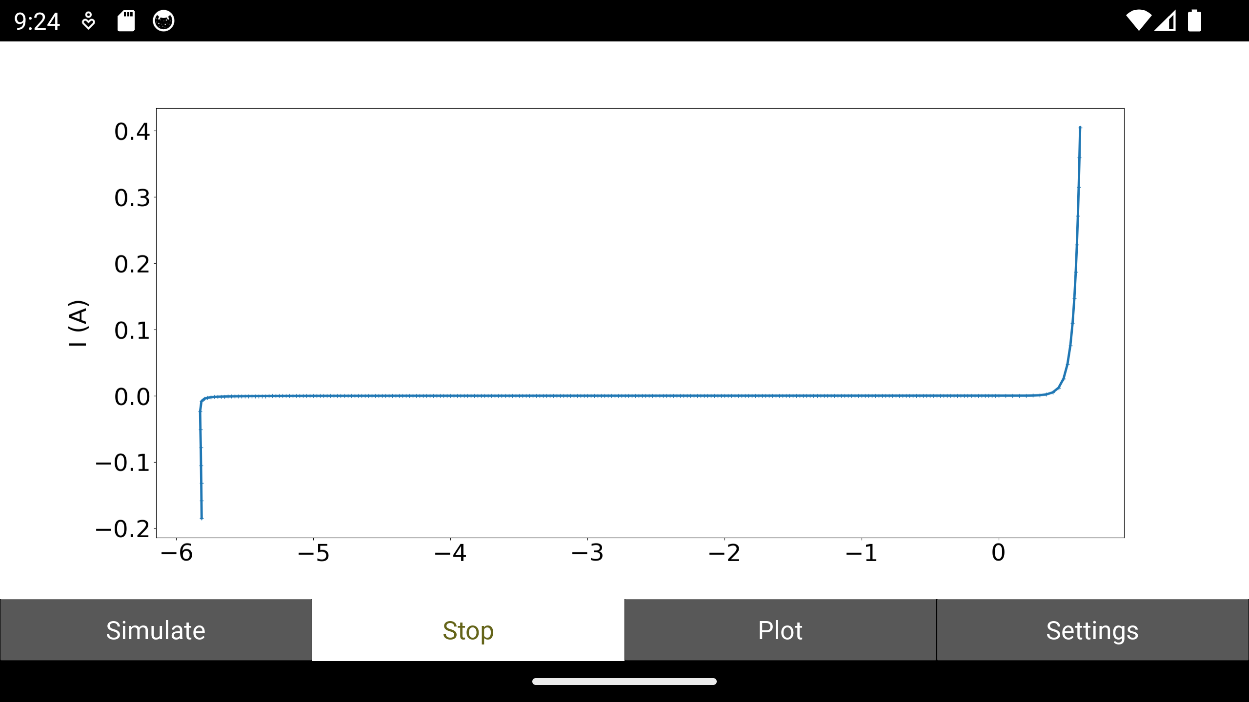
DEVSIM as TCAD mobile app

DEVSIM: TCAD mobile app


Now through January 18, 2024, the TCAD app is free for download. After this, you will be entitled to any free future updates [read more...]

  • App is renamed to “TCAD app”
  • Impact ionization model added
  • Menus updated
  • Easier plot navigation
  • Series resistance available to aid in impact ionization model results
  • Stop simulation and keep partial results to stop long-running simulation early

Get it on Google Play Download on the App Store

[C4P] MIXDES 2024

The MIXDES conference series started in Dębe near Warsaw in 1994 and has been organized yearly in the most interesting Polish cities. In 2024 we would like to continue the tradition of inviting you to the most attractive places in Poland and the conference will take place in Gdańsk between June 27-29, 2024
In short period of time the conference has become an important event in the Central Europe allowing to discuss the recent research progress in the field of design, modelling, simulation, testing and manufacturing in various areas such as micro- and nanoelectronics, semiconductors, sensors, actuators and power devices as well as their interdisciplinary applications.

The topics of the MIXDES 2024 Conference include:
  • Design of Integrated Circuits and Microsystems
    Design methodologies. Digital and analog synthesis. Hardware-software co-design. Reconfigurable hardware. Hardware description languages. Intellectual property-based design. Design reuse.
  • Thermal Issues in Microelectronics
    Thermal and electro-thermal modelling, simulation methods and tools. Thermal mapping. Thermal protection circuits. 
  • Analysis and Modelling of ICs and Microsystems
    Simulation methods and algorithms. Behavioral modelling with VHDL-AMS and other advanced modelling languages. Microsystems modelling. Model reduction. Parameter identification.
  • Microelectronics Technology and Packaging
    New microelectronic technologies. Packaging. Sensors and actuators.
  • Testing and Reliability
    Design for testability and manufacturability. Measurement instruments and techniques. 
  • Power Electronics
    Design, manufacturing, and simulation of power semiconductor devices. Hybrid and monolithic Smart Power circuits. Power integration.
  • Signal Processing
    Digital and analogue filters, telecommunication circuits. Neural networks. Artificial intelligence. Fuzzy logic. Low voltage and low power solutions.
  • Embedded Systems
    Design, verification and applications.
  • Medical Applications
    Medical and biotechnology applications. Biometrics. Thermography in medicine
Call for Papers and Contributions
A call is made for papers, contributions and other conference activities on the topics mentioned above. Full papers should be submitted till March 1, 2024 - only in electronic form (MS Word, RTF, Open Office Writer, LaTeX, together with a generated PDF file).

The paper submission form and required format is available on our Web page. Authors are asked to indicate the topic into which their papers fall. The papers will be reviewed by at least two referees from the International Programme Committee. The papers will be published in the proceedings from the author's electronic submission.

Tutorials and Special Sessions - Call for Proposals
Several tutorials/special sessions will be held prior to the conference. Authors willing to propose a tutorial at MIXDES 2024 are invited to send a proposal to the Organizing Committee. The proposal should consist of a three-page summary including tutorial title, name and affiliation of the lecturer(s), tutorial objectives and audience, topical outline and provisional schedule of the tutorial.

Jan 11, 2024

[paper] Neural Compact Modeling Framework

Eom, Seungjoon, Hyeok Yun, Hyundong Jang, Kyeongrae Cho, Seunghwan Lee, Jinsu Jeong, and Rock‐Hyun Baek
Neural Compact Modeling Framework for Flexible Model Parameter Selection with High Accuracy and Fast SPICE Simulation
Advanced Intelligent Systems (2023): 2300435
DOI: 10.1002/aisy.202300435

Department of Electrical Engineering, Pohang University of Science and Technology, Pohang 37673 (KR)

Abstract: Neural compact models are proposed to simplify device-modeling processes without requiring domain expertise. However, the existing models have certain limitations. Specifically, some models are not parameterized, while others compromise accuracy and speed, which limits their usefulness in multi-device applications and reduces the quality of circuit simulations. To address these drawbacks, a neural compact modeling framework with a flexible selection of technology-based model parameters using a two-stage neural network (NN) architecture is proposed. The proposed neural compact model comprises two NN components: one utilizes model parameters to program the other, which can then describe the current–voltage (IV) characteristics of the device. Unlike previous neural compact models, this two-stage network structure enables high accuracy and fast simulation program with integrated circuit emphasis (SPICE) simulation without any trade-off. The IV characteristics of 1000 amorphous indium–gallium–zinc-oxide thin-film transistor devices with different properties obtained through fully calibrated technology computer-aided design simulations are utilized to train and test the model and a highly precise neural compact model with an average IDS error of 0.27% and R2 DC characteristic values above 0.995 is acquired. Moreover, the proposed framework outperforms the previous neural compact modeling methods in terms of SPICE simulation speed, training speed, and accuracy.

Fig: a) The structure of a-IGZO TFT structure simulated with TCAD
b) Calibrated a-IGZO sub-gap DOS

Acknowledgements: This work was supported in part by the LG Display Company, in part by the Brain Korea 21 Fostering Outstanding Universities for Research (BK21 FOUR) program, in part by Institute of Information and Communications Technology Planning and Evaluation (IITP) grant funded by the Korea government (MSIT) (grant no. 2019-0-01906, Artificial Intelligence Graduate School Program [POSTECH]), in part by the Ministry of Trade, Industry and Energy (MOTIE) under grant no. 20020265, in part by Korea Semiconductor Research Consortium (KSRC) support program for the development of the future semiconductor device, and in part by the Technology Innovation Program (grant no. RS2023-00231985) funded by the Ministry of Trade, Industry and Energy (MOTIE, Korea) (grant no. 1415187390).


[github] new RevEDA Release

Revolution EDA Schematic/Symbol/Layout Editors
https://github.com/eskiyerli/revedaRelease

A new release of Revolution EDA is almost here, including a brand-new hierarchical layout editor with GDS export capability, revamped schematic, and symbol editors. Layout editor can use python-based parametric layout cells. The editor can also create vias and via arrays, paths (Manhattan, diagonal and free-angle), rectangles, polygons, pins and texts. Schematic editor can now import Spice subcircuits and create symbols for inclusion in the schematic editor. A cell can have more than one cellview such as SPICE, Verilog-A or symbol that can be used in the netlisting. The netlisting process can be controlled by a switch-view list or by a separate config view. Unlike leading commercial EDA systems, netlisting and GDS export process are running as separate threads and do not block the user's work.

Any interested parties are kindly invited to get in touch with Murat Eskiyerli, the lead RevEDA developer

[C4P] 82nd DRC

DRC 2024 
The 82nd Device Research Conference
The University of Maryland, College Park


DRC will be held in coordination with the Electronic Materials Conference (EMC), which will occur the same week, from June 26-28. This recognizes the strong interaction between device and electronic materials research and provides fruitful exchanges of information between attendees of both Conferences.

The 2024 Conference will feature:
  • An informative, timely short course in rapidly developing fields
  • Oral and poster presentations on electronic/photonic device experiments 
  • and simulations
  • Plenary and invited presentations given by worldwide leaders
  • Evening rump sessions
  • Strong student participation and Student Paper Awards
  • Focus Sessions on Devices for Neuromorphic Computing
  • More than 50 invited speakers covering a wide spectrum of devices
Topics to be presented include:
  • Devices for Biological and Healthcare Applications
  • Emerging Devices
  • Devices for Extreme Conditions
  • Spintronic and Magnetic Devices
  • Memory Devices
  • Modeling and Simulation of Devices
  • Nanoscale and Vacuum Devices
  • Optoelectronic and Optical Devices
  • Power Devices
  • Quantum Devices
  • Heterogeneously Integrated Devices
  • Thin-Film and Flexible Devices
  • RF and Terahertz Devices
  • Wide-bandgap Device
  • 2D Materials and Devices
  • Neuromorphic Computing Devices
Important Dates
  • Feb. 16, 2024 Abstract Submission Deadline
  • April 5, 2024 Acceptance Notification
  • April 10, 2024 Registration Opens
  • May 15, 2024 Early Bird Registration Deadline

Jan 8, 2024

[paper] OTA using the Open Sky130 PDK

Carolina Vieira Souza, Edmar Philipe Ribeiro
and Estêvao Coelho Teixeira
Design of a Linear Transconductance OTA using the Open Sky130 Process Design Kit
Sociedade Brasileira De Microeletrônica
(2023) sbmicro.org.br
doi: 10.5281/zenodo.10646550

Faculdade de Engenharia, Universidade Federal de Juiz de Fora, Brazil

Abstract: This paper describes the design, layout and simulation of a linear transconductance Operational Transconductance Amplifier (OTA) using the SkyWater 130nm open Process Design Kit (PDK). By using a known source degeneration technique, it is possible to either decrease and linearize the transconductance of the OTA for a wider range of input voltages, making it proper for use on Gm-C filters. Only open source tools, suited for the Sky130 PDK, were used in this design, showing the applicability to analog designs.

Fig: Linear OTA Structure: (a) Complete circuit, with source degeneration resistors;
(b) Alternative source degeneration triode MOSFETs; and its GDSII layout, with identification of some relevant parts: (A) differential pair; (B) source-degeneration resistors; (C) biasing transistors.

Acknowledgment: This work is result from a scientific initiation project covered by the VI VIC 2022/2023 Program, by PROPP/UFJF.


[paper] Polylogarithms in MOSFET Modeling

A. Ortiz-Conde and F. J. García-Sánchez
Recent Applications of Polylogarithms in MOSFET Modeling
2023 IEEE 33rd International Conference on Microelectronics
MIEL, Nis, Serbia, 2023, pp. 1-8
DOI: 10.1109/MIEL58498.2023.10315897

Department of Electronics and Circuits, Universidad Simón Bolívar, Caracas, Venezuela

Abstract: We present a review of recent uses of the special mathematical function known as the polylogarithm for MOSFET modeling applications. We first summarize some basic properties of polylogarithms, with a particular focus on those with negative exponential argument. After examining cases of the use of first order polylogarithms pertinent to electron device modeling, we explain the reasons that motivate the use of polylogarithms of diverse orders for formulating mono- and poly-crystalline succinct compact MOSFET models. We then analyze a particular representative example: the modeling of polysilicon MOSFETs using the polylogarithm. Recalling that polylogarithms may be used to faithfully represent Fermi-Dirac Integrals in general, and considering that they are analytically differentiable and integrable, we describe a full Fermi–Dirac Statistics-based version of the usually approximate Boltzmann Statistics-based MOSFET Surface Potential Equation (SPE).

TABLE: Some Features of Polylogarithms with Negative Exponential Argument


[paper] Compact Model of Graphene FETs

Nikolaos Mavredakis, Anibal Pacheco-Sanchez, Oihana Txoperena,
Elias Torres, and David Jiménez
A Scalable Compact Model for the Static Drain Current of Graphene FETs
IEEE TED, Vol. 71, No. 1, January 2024
DOI:  10.1109/TED.2023.3330713

1 Departament d’Enginyeria Electrònica, Escola d’Enginyeria, UAB, 08193 Bellaterra, Spain
2 Graphenea Semiconductor SLU, 20009 San Sebastián, Spain.

Abstract: The main target of this article is to propose for the first time a physics-based continuous and symmetric compact model that accurately captures I–V experimental dependencies induced by geometrical scaling effects for graphene field-effect transistor (GFET) technologies. Such a scalable model is an indispensable ingredient for the boost of large-scale GFET applications, as it has been already proved in solid industry-based CMOS technologies. Dependencies of the physical model parameters on channel dimensions are thoroughly investigated, and semi-empirical expressions are derived, which precisely characterize such behaviors for an industry-based GFET technology, as well as for others developed in the research laboratory. This work aims at the establishment of the first industry standard GFET compact model that can be integrated in circuit simulation tools and, hence, can contribute to the update of GFET technology from the research level to massive industry production.

Fig: Graphenea GFET schematic cross-section not drawn to scale. Graphene under metal contacts is not shown.The drain current has explicit derivation in respect to Qgr, where Qt and Qp(n) are the transport sheet and p(n)-type charges, respectively; Vc is the chemical potential, h is the reduced Planck constant, uf is the Fermi velocity, e is the electron charge, and k is a coefficient. Qt and, thus, ID can be calculated according to Vc polarity at source (Vcs) and drain (Vcd), respectively. Hence, at n-type region where Vcs, Vcd > 0 and Qp = 0

Acknowledgements: This work was supported in part by the European Union’s Horizon 2020 Research and Innovation Program GrapheneCore3 under Grant 881603; in part by the Ministerio de Ciencia, Innovación y Universidades under Grant RTI2018-097876-B-C21 (MCIU/AEI/ FEDER, UE), Grant FJC2020-046213-I, and Grant PID2021-127840NBI00 (MCIN/AEI/FEDER, UE); in part by the European Union Regional Development Fund within the Framework of the ERDF Operational Program of Catalonia 2014–2020 with the Support of the Department de Recerca i Universitat, with a grant of 50% of Total Cost Eligible; and in part by the GraphCAT Project under Grant 001-P-001702. 

Jan 5, 2024

ISHI-kai January 2024 event

2024年1月イベント「オープンソースPDK団体」勉強会国内外のオ
ープンソースPDKやEDAの状況について、キーマンに語っていただきます
With the recent rise in the semiconductor industry, the movement of open source PDK and EDA in Japan and overseas has become active. Therefore, in this study session, key people will talk about the status of open source PDK and EDA in Japan and overseas.

Schedule
Friday, January 26, 2024, 18:00-21:00 (Reception: 18:30)

Venue (onsite)
Google Shibuya Office
3-21-3 Shibuya, Shibuya-ku, Tokyo
Shibuya Stream Google reception meeting

Online Broadcast: 
Google Meet: https://meet.google.com/ksa-tjaw-ges

Participation Fee
free
Timetable
TimeSpeakerTitleLecture Outline
Until 18:30ISHI-kaireceptionThe entrance to the facility closes at this time, so if you are participating locally, please come by this time as much as possible.
18:00 ~ 18:30ISHI-kaiChat time-
18:30 ~ 19:15 (Lecture: 30min, Q&A: 15min)Takeshi Hamamoto
Minimal Fab Propulsion Organization Device Engineer 
minimal Fab open PDK1) What is a minimal fab
2) openPDK
3) Design Contest at Semicon 2023

19:15 ~ 20:00 (Lecture: 30min., Q&A: 15min.)Junichi Okamura
IEEE Senior Member 
OpenPDK and the World-
20:00 ~ 20:45 (Lecture: 30min., Q&A: 15min.)@noritsunaAbout the upcoming open source PDK shuttle(To be released at a later date)
21:00ISHI-kaiclosing

What is ISHI-kai?
The association was named ISHI-kai (Inter-linked Society on Homemade IC Kai). The name was conceived from the Society Community (Association) that handles open (democratized) ISHI = stone = Silicon = semiconductors (ASIC/LSI/IC) and connects various fields.

OpenMPW (Open Multi Project Wafer), which appeared as a forerunner, is a shuttle program created by Google investing in Efabless, and includes the tools necessary for making semiconductors (ASIC/LSI/IC) (EDA/PDK) to ISHI manufacturing in IC fabs). This is exactly the "openness of semiconductors (ASIC/LSI/IC) and EDA/PDK" of the open source movement (democratization of software) that started with GNU!

Therefore, this association was established as a user society community (association) that focuses not only on experts in semiconductors (ASIC/LSI/IC) in the past, but also on those who see the potential of the open source movement of semiconductors (ASIC/LSI/IC) in the future and those who want to create new semiconductors (ASIC/LSI/IC).

We/ISHI-kai will continue to work toward a world where semiconductors (ASIC/LSI/IC) and EDA/PDK can be used by everyone, just as OSs, compilers, libraries, apps, electronic boards, 3D CAD and 3D printers that we/ISHI-kaire only available to experts can now be used by everyone as open source software, open hardware, open modeling, etc.

As for the future activity plan, we/ISHI-kai have a policy of revolutionizing the semiconductor (ASIC/LSI/IC) field by involving people from other fields, and we/ISHI-kai will hold events such as hands-on seminars for ultra-beginners for other fields and in-depth study sessions for experts, form a team to challenge the OpenMPW shuttle and Chipathon from around the world, and Maker we/ISHI-kai would like to participate in events such as Faire, so thank you.

Precautions
As events move online, we/ISHI-kai ask participants to act in accordance with the spirit of the Code of Conduct. If you have any problems, please contact the organizer. If it is judged that there is no improvement in the request even if there is no abuse such as vandalism or malicious intent, we/ISHI-kai may respond on a case-by-case basis. 
https://www.contributor-covenant.org/ja/version/2/0/code_of_conduct/

Acknowledgements
Thanks to the kindness of Google for providing a real/onsite venue.

Jan 3, 2024

VLSID 2024 Conference


PULP Platform @pulp_platform (5h)
Cheers to 2024! The 37th International Conference on VLSI Design will start in Kolkata on Monday. @LucaBenini will give a banquet talk titled "Open Platform for the Embodied AI Era" at 7:10 PM (IST) on January 9. Check out the conference website for tutorials and schedule: https://vlsid.org

In the present era of automation and connected things, VLSI technology armed with AI and Quantum could be pivotal in changing the VLSI landscape starting from manufacturing to devices to design. To elaborate on this paradigm shift, the theme 2024 VLSI Design conference is aptly chosen to be “VLSI meets AI and Quantum for Cyber Physical Systems”.

Over a span of five-days of VLSID2024, the summit will feed brains and nurture minds with state-of-the-art exhibitors, presentations, panel discussions, innovation forums, and tutorials by established technologists.

[paper] MEMS pressure sensors

Xiangguang Han, Mimi Huang, Zutang Wu, Yi Gao, Yong Xia, Ping Yang, Shu Fan, Xuhao Lu, Xiaokai Yang, Lin Liang, Wenbi Su, Lu Wang, Zeyu Cui, Yihe Zhao, Zhikang Li, Libo Zhao
and Zhuangde Jiang
Advances in high-performance MEMS pressure sensors: design, fabrication, and packaging.
Microsyst Nanoeng 9, 156 (2023) 
DOI:10.1038/s41378-023-00620-1

1 State Key Laboratory for Manufacturing Systems Engineering, Xi’an Jiaotong University, Xi’an 710049, China
2 International Joint Laboratory for Micro/Nano Manufacturing and Measurement Technologies, Xi’an Jiaotong University, Xi’an 710049, China.
3 School of Mechanical Engineering, Xi’an Jiaotong University, Xi’an 710049, China.
4 Northwest Institute of Nuclear Technology, Xi’an 710024, China


Abstract: Pressure sensors play a vital role in aerospace, automotive, medical, and consumer electronics. Although microelectromechanical system (MEMS)-based pressure sensors have been widely used for decades, new trends in pressure sensors, including higher sensitivity, higher accuracy, better multifunctionality, smaller chip size, and smaller package size, have recently emerged. The demand for performance upgradation has led to breakthroughs in sensor materials, design, fabrication, and packaging methods, which have emerged frequently in recent decades. This paper reviews common new trends in MEMS pressure sensors, including minute differential pressure sensors (MDPSs), resonant pressure sensors (RPSs), integrated pressure sensors, miniaturized pressure chips, and leadless pressure sensors. To realize an extremely sensitive MDPS with broad application potential, including in medical ventilators and fire residual pressure monitors, the “beam-membrane-island” sensor design exhibits the best performance of 66 μV/V/kPa with a natural frequency of 11.3 kHz. In high-accuracy applications, silicon and quartz RPS are analyzed, and both materials show ±0.01%FS accuracy with respect to varying temperature coefficient of frequency (TCF) control methods. To improve MEMS sensor integration, different integrated “pressure + x” sensor designs and fabrication methods are compared. In this realm, the intercoupling effect still requires further investigation. Typical fabrication methods for microsized pressure sensor chips are also reviewed. To date, the chip thickness size can be controlled to be <0.1 mm, which is advantageous for implant sensors. Furthermore, a leadless pressure sensor was analyzed, offering an extremely small package size and harsh environmental compatibility. This review is structured as follows. The background of pressure sensors is first presented. Then, an in-depth introduction to MEMS pressure sensors based on different application scenarios is provided. Additionally, their respective characteristics and significant advancements are analyzed and summarized. Finally, development trends of MEMS pressure sensors in different fields are analyzed.

Fig: High-sensitivity MDPS, on-chip amplified MDPS, and resonant MDPS.

Acknowledgements: This study was supported in part by the National Key Research and Development Program of China (2021YFB3203200) and the Natural Scienc Foundation of Shaanxi (2022JQ-554).