Feb 28, 2020

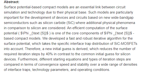
#paper: M. Albrecht, F. J. Klüpfel and T. Erlbacher, "An Iterative Surface Potential Algorithm Including Interface Traps for Compact Modeling of SiC-MOSFETs," in IEEE TED, vol. 67, no. 3, pp. 855-862, March 2020 doi: 10.1109/TED.2020.2967507 https://t.co/8fJMfKM9SP https://t.co/nlRiSs1Qf0


from Twitter https://twitter.com/wladek60

February 28, 2020 at 06:12PM
via IFTTT

Feb 25, 2020

#paper: Thomas, S. Guiding the design of #negative-#capacitance #FETs. Nat Electron 3, 72 (2020). https://t.co/clMVy6syW9 https://t.co/zh8N3ynGIx https://t.co/s3KFFkQ8lT


from Twitter https://twitter.com/wladek60

February 25, 2020 at 02:57PM
via IFTTT

#Opensource licenses: What, which, and why https://t.co/kZlEUC5CQE https://t.co/G1WotNhQp8


from Twitter https://twitter.com/wladek60

February 25, 2020 at 09:42AM
via IFTTT

Fwd: IEEE-EDS Santa Clara Valley/San Francisco Chapter March Seminar

We are pleased to announce our monthly seminar for March

Wide Bandgap Devices Enabling High Power and High Frequency Electronics

Speaker: Professor Srabanti Chowdhury, Stanford University

Friday, March 13, 2020 at 11:45AM – 1PM

Texas Instruments Conference Center
2900 Semiconductor Dr, Building E, Santa Clara, CA 95051
FREE PIZZA PROVIDED

Register Here: https://www.surveymonkey.com/r/R7VKQ3M

Abstract:
We live in extremely exciting times, often identified as the age of the fourth industrial revolution. With electrification at every level, we are witnessing the most significant transformation of transportation since the internal combustion engine. Renewable energy is now a reality. IoT with the ever-expanding need for sensors and low power electronics is changing our lives dramatically. Robotics and autonomous vehicles are upon us. Both new and existing applications are demanding physical electronics solutions with new materials, devices and heterogeneous integration to drive these innovations to their full potential.

Wide-bandgap (WBG) semiconductors present a pathway to enable much of these electronics with higher efficiency and newer functionalities. Semiconductor devices with higher power density have unprecedented value in both power and high frequency electronics. Reducing conversion losses is not only critical for minimizing consumption of limited resources, it simultaneously enables new compact and reduced weight solutions, the basis for a new industry offering increased power conversion performance at reduced system cost. Equally importantly, GaN has opened the door to other ultra-wide bandgap materials such as Diamond, Aluminum Nitride and Gallium Oxide.


More information at the IEEE EDS Santa Clara Valley-San Francisco Chapter Home Page

Subscribe or Invite your friends to sign up for our mailing list and get to hear about exciting electron-device relevant talks. We promise no spam and try to minimize email. You can unsubscribe easily.
http://site.ieee.org/scv-eds/subscribe/

[mos-ak] [Final Program] 2nd Latin America MOS-AK Workshop at LAEDC

2nd Latin America MOS-AK Workshop at LAEDC
(co-located with LAEDC /LASCAS)
Escazu, Costa Rica, February 25, 2020

Today, Professor Benjamin Iniguez URV, DEEEA, Tarragona, (SP) on behalf of the Extended MOS-AK TPC Committee will open 2nd consecutive Latin America MOS-AK Workshop

Scheduled, 2nd consecutive Latin America MOS-AK Workshop co-located with LAEDC /LASCAS aims to strengthen a network and discussion forum among experts in the field, enhance open platform for information exchange related to compact/SPICE modeling and Verilog-A standardization, bring people in the compact modeling field together, as well as obtain feedback from technology developers, circuit designers, and TCAD/EDA tool developers and vendors.
 
The MOS-AK workshop program is available online:
<http://www.mos-ak.org/costa_rica_2020/>

Venue:
Escazu, west of San José, 
Costa Rica

Online Registration is still open
(any related enquiries can be sent to register@mos-ak.org)

Postworkshop Publications:
Selected best MOS-AK technical presentation will be recommended for further publication
in a special 
Solid State Electronics issue on compact modeling 

W.Grabinski on behalf of International MOS-AK Committee
WG25022020

--
You received this message because you are subscribed to the Google Groups "mos-ak" group.
To unsubscribe from this group and stop receiving emails from it, send an email to mos-ak+unsubscribe@googlegroups.com.
To view this discussion on the web visit https://groups.google.com/d/msgid/mos-ak/e3973eec-ace1-4649-8f32-cf116448a002%40googlegroups.com.