Showing posts with label spice. Show all posts

Apr 26, 2022

[paper] Universal Charge Model for Multigate MOS Structures

Kwang-Woon Lee and Sung-Min Hong
Derivation of a Universal Charge Model for Multigate MOS Structures
with Arbitrary Cross Sections
IEEE TED (2022, Early Access)
DOI:  10.1109/TED.2022.316486
   
* Gwangju Institute of Science and Technology (KR)

Abstract: A universal equation for the charge-voltage characteristics in the multigate metal oxide semiconductor (MOS) structure with an arbitrary cross section is presented. A generalized coordinate is proposed and the Poisson equation is integrated with a weighting factor related with the generalized coordinate and the electric field. A compact charge model is derived and analytic and numerical examples for various MOS structures are shown.
Fig: Thin slab in the semiconductor channel region of the multigate MOS structure. The A∗ surfaces are perpendicular to the z-direction, which is the transport direction and its generalized coordinate, ψ, for rectangular nanosheet MOS structures at 0.0 V (top) and 0.7 V (bottom).

Aknowlegements: This workwas supported by the National Research Foundation of Korea (NRF) Grant funded by the Korean Government under Grant NRF- 2019R1A2C1086656 and Grant NRF-2020M3H4A3081800.

[paper] DL Physics-Driven MOSFET Modeling

Ming-Yen Kao, H. Kam, and Chenming Hu, Life Fellow, IEEE
Deep-Learning-Assisted Physics-Driven MOSFET Current-Voltage Modeling
in IEEE Electron Device Letters
DOI: 10.1109/LED.2022.3168243

Abstract: In this work, we propose using deep learning to improve the accuracy of the partially-physics-based conventional MOSFET current-voltage model. The benefits of having some physics-driven features in the model are discussed. Using a portion of the Berkeley Short-channel IGFET Common-Multi-Gate (BSIM-CMG), the industry-standard FinFET and GAAFET compact model, as the physics model and a 3-layer neural network with 6 neurons per layer, the resultant model can well predict IV, output conductance, and transconductance of a TCAD-simulated gate-all-around transistor (GAAFET) with outstanding 3-sigma errors of 1.3%, 4.1%, and 2.9%, respectively. Implications for circuit simulation are also discussed.
Fig: (a) Model implementation for circuit simulations, without the relative gm and gds errors terms in the cost function, Model shows larger prediction error in (b) gm and (c) gds.

Acknowledgements: This work was supported by the Berkeley Device Modeling Center, 
UCB, CA (USA)


Mar 1, 2022

[paper] Multi-Segment TFT Compact Model for THz Applications

Xueqing Liu1,Trond Ytterdal2 and Michael Shur1,3
Multi-Segment TFT Compact Model for THz Applications
Nanomaterials 2022, 12(5), 765; 
DOI: 10.3390/nano12050765
  
1 RPI, Troy, NY 12180, USA
2 Norwegian University of Science and Technology, Trondheim, Norway
3 Electronics of the Future, Inc., USA

Abstract: We present an update of the Rensselaer Polytechnic Institute (RPI) thin-film transistor (TFT) compact model. The updated model implemented in Simulation Program with Integrated Circuit Emphasis (SPICE) accounts for the gate voltage-dependent channel layer thickness, enables the accurate description of the direct current (DC) characteristics, and uses channel segmentation to allow for terahertz (THz) frequency simulations. The model introduces two subthreshold ideality factors to describe the control of the gate voltage on the channel layer and its effect on the drain-to-source current and the channel capacitance. The calculated field distribution in the channel is used to evaluate the channel segment parameters including the segment impedance, kinetic inductance, and gate-to-segment capacitances. Our approach reproduces the conventional RPI TFT model at low frequencies, fits the measured current–voltage characteristics with sufficient accuracy, and extends the RPI TFT model applications into the THz frequency range. Our calculations show that a single TFT or complementary TFTs could efficiently detect the sub-terahertz and terahertz radiation.
FIG: (a) quivalent circuit of the multi-segment SPICE model for TFT and
(b) equivalent circuit for each segment including leakage components

Acknowledgements: The work was supported by Office of Naval Research (N000141712976, Project Monitor Paul Maki).

Feb 9, 2022

[paper] SPICE simulation of PIN diodes and IGBT devices

Manhong Zhang, Yi Zhai
Recovering the carrier number conservation in SPICE simulation of PIN diodes and IGBT devices
Solid-State Electronics
Available online 7 February 2022, 108239
DOI: 10.1016/j.sse.2022.108239
   
North China Electric Power University, Beijing 102206, China


Abstract: In SPICE simulations of PIN diodes and IGBT devices using finite difference method, one discretizes an undepleted N- region into several equally spaced nodes with a time-dependent distance of Δx(t). Then transforms the ambipolar diffusion equation, a time-space partial differential equation, into a set of time-dependent ordinary differential equations. However, the time-dependent property of Δx(t) destroys the carrier number conservation. In this paper, we propose an approach to account for the effect of the Δx(t) by introducing an auxiliary system. It has the same total current and the total carrier number in the undepleted N- region as the real system, but has different electron and hole current components. The difference is caused by adding compensation current terms with the equal amplitude and opposite sign to the electron and hole current terms in the auxiliary system. These compensation current terms are proportional to the boundary speed of the undepleted N- region and do not change the total current. The auxiliary system can be easily solved using SPICE behavior models and its carrier density is a good approximation to the real one. Our simulations show that the compensation current correction is important for fast switching PIN diodes, but may not be very important in IGBT devices due to their large gate-related capacitance.
FIG: SPICE simulation model of PIN diodes and IGBT devices

Jan 5, 2022

[book] Advanced ASM-HEMT Model for GaN HEMTs

Sourabh Khandelwal
Advanced SPICE Model for GaN HEMTs (ASM-HEMT)
A New Industry-Standard Compact Model 
for GaN-based Power and RF Circuit Design
DOI: 10.1007/978-3-030-77730-2
eBook ISBN: 978-3-030-77730-2

Describes in detail a new industry standard for GaN-based power and RF circuit design. Includes discussion of practical problems and their solutions in GaN device modeling. Covers both radio-frequency (RF) and power electronics application of GaN technology and describes SPICE modeling of both GaN RF and power devices.


Table of contents:

  • Front Matter; pp. i-xv
  • Gallium Nitride Semiconductor Devices; pp. 1-8
  • Compact Modeling; pp. 9-19
  • Introduction to ASM-HEMT Compact Model; pp. 21-31
  • Core Formulations in ASM-HEMT Model; pp. 33-45
  • Non-ideal Effects in Device Current and Their Modeling; pp. 47-62
  • Trapping Models; pp. 63-81
  • Non-Ideal Effects in GaN Capacitances and Their Modeling; pp. 83-100
  • Gate Current Model; pp. 101-113
  • Effect of Ambient Temperature on GaN Device; pp. 115-124
  • Noise Models; pp. 125-130
  • Parameter Extraction in ASM-HEMT Model; pp. 131-150
  • Advance Simulations with ASM-HEMT Model; pp. 153-174
  • Resources for ASM-HEMT Model Users; pp. 175-175
  • Back Matter; pp. 175-188

About the author:
Sourabh Khandelwal is Senior Lecturer at the School of Engineering at Macquarie University, Sydney. He is the lead developer of ASM--HEMT compact model, which is a new industry standard compact model for GaN RF and power devices. Earlier to this role, Manager of Berkeley Device Modeling Center and Postdoctoral Researcher at the BSIM group at University of California, Berkeley. Before that, he worked as Research Engineer at IBM Semiconductor Research. He has over 200 publications in top-tier conferences and journals in the area of semiconductor device modeling and circuit design.

Dec 8, 2021

Guardian of Verilog-A Compact Models


on 02/02/2020, Geoffrey Coram, Staff CAD Engineer at Analog Devices and Verilog-A Recommended Practices CMC Chair was honored by Prof. Chenming Hu and the BSIM Group at UC Berkeley, naming him as "Guardian of Verilog-A Compact Models for the Global Semiconductor Industry"

Nov 9, 2021

8th EuroSOI-ULIS 2022 at University of Udine (Italy)

Organized by:
University of Udine (Italy)

Conference chair:
Pierpaolo Palestri

Local organizing Committee:
Francesco Driussi
David Esseni
Daniel Lizzit

Conference Secretariat:
Centro Congressi Internazionali 

Steering Committee:
  • Francis BALESTRA
    (IMEP Minatec, France)
  • Maryline BAWEDIN
    (IMEP-LAHC, France)
  • Cor CLAEYS
    (KU-Leuven, Belgium)
  • Bogdan CRETU
    (ENSICAEN, France)
  • Sorin CRISTOLOVEANU
    (IMEP-LAHC, France)
  • Francisco GAMIZ
    (UnivGranada, Spain)
  • Elena GNANI
    (Univ. of Bologna, Italy)
  • Benjamin INIGUEZ 
    (URV, Spain)
  • Joris LACORD
    (CEA-Leti, France)
  • Enrico SANGIORGI
    (Univ.Bologna, Italy)
  • Luca SELMI
    (Univ. of Modena, Italy)
  • Viktor SVERDLOV
    (TU Wien, Austria)
  • Andrei VLADIMIRESCU
    (ISEP, France)
Sponsors:


8th Joint International EuroSOI Workshop and International Conference
on Ultimate Integration on Silicon (EuroSOI-ULIS) 2022
May 18-20, 2022 – Udine, Italy

https://eurosoiulis2022.com

The Conference aims at gathering together scientists and engineers working in academia, research centers and industry in the field of SOI technology and nanoscale devices in More-Moore and More-Than-Moore scenarios. High quality contributions in the following areas are solicited:
  • Advanced SOI materials and structures, innovative SOI-like devices.
  • Alternative transistor architectures (FDSOI, Nanowire, FinFET, MuGFET, vertical MOSFET, FeFET and TFET, MEMS/NEMS, Beyond-CMOS).
  • New channel materials for CMOS (strained Si/Ge, III-V, carbon nanotubes; graphene and other 2D materials).
  • Properties of ultra-thin semiconductor films and buried oxides, defects, interface quality; thin gate dielectrics: high-κ and ferroelectric materials for switches and memory.
  • New functionalities and innovative devices in the More than Moore domain: nanoelectronic sensors, biosensor devices, energy harvesting devices, RF devices, imagers, integrated photonics (on SOI), etc.
  • Transport phenomena, compact modeling, device simulation, front- and back-end process simulation.
  • CMOS scaling perspectives; device/circuit level performance evaluation; switches and memory scaling; three-dimensional integration of devices and circuits, heterogeneous integration.
  • Advanced test structures and characterization techniques, parameter extraction, reliability and variability assessment techniques for new materials and novel devices.
Original 2-page abstracts with illustrations will be reviewed by the Scientific Committee. The accepted contributions will be published as 4-page letters in a special issue of the Elsevier journal Solid-State Electronics. Extended versions of outstanding papers will be published in a further special issue of Solid-State Electronics. A best poster award will be attributed by ELSEVIER. 

The “Androula Nassiopoulou Best Paper Award"
will be attributed by the SINANO institute.

Important dates:
  • abstract submission deadline: March 1, 2022
  • notification of acceptance: March 15, 2022

Oct 26, 2021

conference paper reached 400 reads

conference paper reached 400 reads

Bucher, M., J-M. Sallese, F. Krummenacher, D. Kazazis, C. Lallement, W. Grabinski, and C. Enz
EKV 3.0: An analog design-oriented MOS transistor model
In 9th International Conference on Mixed Design of Integrated Circuits and Systems
(MIXDES 2002)

Abstract:  The EKV 3.0 compact MOS transistor model for advanced analog IC design and simulation is presented. The model is based on the surface potential approach combined with inversion charge linearization. The ideal long-channel model is coherent  for  static  and  dynamic  aspects  including  noise.  The  ideal  model  is  extended  for  high-field  effects  in  deep submicron CMOS technologies. Scalability over channel length and width is achieved while retaining a reduced number of parameters. The EKV 3.0 model is applicable over a large range of CMOS technologies.  

Fig: Normalized source transconductance to current ratio (gm/ID) vs. normalized current, measured 
(markers) in saturation from various CMOS technologies, and analytical model.


Oct 7, 2021

[paper] Compact Schottky-barrier CNTFET Modeling

Manojkumar Annamalai and Michael Schroter
Compact formulation for the bias dependent quasi-static mobile charge in Schottky-barrier CNTFETs IEEE Transactions on Nanotechnology (2021)
DOI: 10.1109/TNANO.2021.3116694

CEDIC, Technische Universität Dresden (D)

Abstract: Carbon nanotube (CNT) field-effect transistors (FETs) are promising candidates for future high-frequency (HF) system-on-chip applications. Understanding and modeling mobile charge storage on CNTs is therefore essential for device optimization and circuit design. A physics-based compact analytical formulation is presented that enables an accurate approximation of the mobile charge in Schottky-barrier CNTFETs over the practically relevant bias range for HF circuit design. The formulation is C∞ continuous and yields accurate results also for the capacitances. The new formulation has been verified for both ballistic and scattering dominated carrier transport by employing device simulation, which was calibrated to experimental data from multi-tube CNTFETs.

Fig: Band diagram in a CNTFET along the axial direction (left red arrow) and, with applied gate bias, along the radial direction perpendicular to the gate (right blue arrow).

Acknowledgments: The authors would like to thank Dr. S. Mothes, formerly with CEDIC, for valuable discussions regarding the device simulator. This project was financially supported in part by the German National Science Foundation (DFG SCHR695/6-2).  

Oct 4, 2021

[paper] Flexible Megahertz Organic Transistors

Jakob Leise1,4, Jakob Pruefer1,4, Ghader Darbandy1, Aristeidis Nikolaou1,4, Michele Giorgio2, Mario Caironi2, Ute Zschieschang3, Hagen Klauk3, Alexander Kloes1, Benjamin Iñiguez4
and James W. Borchert5
Flexible megahertz organic transistors and the critical role of the device geometry on their dynamic performance
Journal of Applied Physics 130, 125501 (2021); 
DOI: 10.1063/5.0062146
  
1NanoP, TH Mittelhessen University of Applied Sciences, Gießen 35390, Germany
2Center for Nano Science and Technology @PoliMi, Istituto Italiano di Tecnologia, Milano 20133, Italy
3Max Planck Institute for Solid State Research, Stuttgart 70569, Germany
4DEEA, Uniersitat Rovira i Virgili, Tarragona 43007, Spain
5Georg August University of Goettingen, Goettingen 37077, Germany

  
Abstract: The development of organic thin-film transistors (TFTs) for high-frequency applications requires a detailed understanding of the intrinsic and extrinsic factors that influence their dynamic performance. This includes a wide range of properties, such as the device architecture, the contact resistance, parasitic capacitances, and intentional or unintentional asymmetries of the gate-to-contact overlaps. Here, we present a comprehensive analysis of the dynamic characteristics of the highest-performing flexible organic TFTs reported to date. For this purpose, we have developed the first compact model that provides a complete and accurate closed-form description of the frequency-dependent small-signal gain of organic field-effect transistors. The model properly accounts for all relevant secondary effects, such as the contact resistance, fringe capacitances, the subthreshold regime, charge traps, and non-quasistatic effects. We have analyzed the frequency behavior of low-voltage organic transistors fabricated in both coplanar and staggered device architectures on flexible plastic substrates. We show through S-parameter measurements that coplanar transistors yield more ideal small-signal characteristics with only a weak dependence on the overlap asymmetry. In contrast, the high-frequency behavior of staggered transistors suffers from a more pronounced dependence on the asymmetry. Using our advanced compact model, we elucidate the factors influencing the frequency-dependent small-signal gain and find that even though coplanar transistors have larger capacitances than staggered transistors, they benefit from substantially larger transconductances, which is the main reason for their superior dynamic performance.
Fig: Schematic cross-section of a top-contact (TC) organic TFT. Here, the semiconductor layer separates the source and drain contacts from the gate dielectric and thus from the gate-field-induced charge-carrier channel; hence, these transistors are also referred to as staggered TFTs. The overlap regions are assumed as a series connection of two capacitances. However, when the organic semiconductor (OSC) is operated in accumulation, the accumulation charges change the behavior of the series connection. The charge density at the source end of the channel is assumed to be found in the entire gate-to-source overlap region. 

Acknowledgments: The authors thankfully acknowledge funding for this project from the German Federal Ministry of Education and Research (“SOMOFLEX,” No. 13FH015IX6) and EU H2020 RISE (“DOMINO,” No. 645760), and the German Research Foundation (DFG) under Grant Nos. KL 1042/9-2, KL 2223/6-1, and KL 2223/6-2 (SPP FFlexCom). The authors would like


Jul 13, 2021

[paper] ML based Aging-Aware FPGA Framework

Behnam Ghavami, Milad Ibrahimipour, Zhenman Fang, Lesley Shannon 
MAPLE: A Machine Learning based Aging-Aware FPGA Architecture Exploration Framework
31st International Conference on Field-Programmable Logic and Applications
(FPL 2021 Short Paper),
Virtual Conference, Sept 2021
*Simon Fraser University, Burnaby, BC, Canada

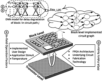
Abstract: In this paper, we develop a framework called MAPLE to enable the aging-aware FPGA architecture exploration. The core idea is to efficiently model the aging-induced delay degradation at the coarse-grained FPGA basic block level using deep neural networks (DNNs). For each type of the FPGA basic block such as LUT and DSP, we first characterize its accurate delay degradation via transistor-level SPICE simulation under a versatile set of aging factors from the FPGA fabric and in-field operation. Then we train one DNN model for each block type to quickly and accurately predict the complex relation between its delay degradation and comprehensive aging factors. Moreover, we integrate our DNN models into the widely used Verilog-to-Routing toolflow (VTR 8) to support analyzing the impact of aging-induced delay degradation on the entire large scale FPGA architecture. Experimental results demonstrate that MAPLE can predict the delay degradation of FPGA blocks 104 to 107 times faster than transistor-level SPICE simulation, with a prediction error less than 0.7%. Our case study demonstrates that FPGA architects can effectively leverage MAPLE to explore better aging-aware FPGA architectures.

Fig: Overview of FPGA fabric and in-field factors affecting FPGA aging at transistor and basic block levels. We use DNNs to model FPGA delay degradation at basic block level.

Acknowledgements: We acknowledge the support from Government of Canada Technology Demonstration Program and MDA Systems Ltd; NSERC Discovery Grant RGPIN-2019-04613 and DGECR 2019-00120; Canada Foundation for Innovation John R. Evans Leaders Fund; Simon Fraser University New Faculty Start-up Grant; Xilinx, Huawei and Nvidia.

Jul 1, 2021

[papers] Compact/SPICE Modeling

[1] M. S. Tarkov; Two-Gate FeFET SPICE Model and Its Application to Construction of Adaptive Adder; 2021 Ural Symposium on Biomedical Engineering, Radioelectronics and Information Technology (USBEREIT), 2021, pp. 0206-0209,
DOI: 10.1109/USBEREIT51232.2021.9455091.

[2] L. Liu, Y. Tian and W. Huang, "A Bio-IA with Fast Recovery and Constant Bandwidth for Wearable Bio-Sensors," in IEEE Sensors Journal,
DOI: 10.1109/JSEN.2021.3092001.

[3] C. -T. Tung, H. -Y. Lin, S. -W. Chang and C. -H. Wu, "Analytical modeling of tunnel-junction transistor lasers," in IEEE Journal of Selected Topics in Quantum Electronics,
DOI: 10.1109/JSTQE.2021.3090527.

[4] Subir Kumar Maity, Soumya Pandit; A SPICE compatible physics-based intrinsic charge and capacitance model of InAs-OI-Si MOS transistor, Superlattices and Microstructures, Volume 156, 2021, 106975, ISSN 0749-6036,
DOI: 10.1016/j.spmi.2021.106975

Fig:  Strucutre of InAs-OI-Si MOS transistor


Jun 11, 2021

[paper] SPICE Modeling of Cycle-to-Cycle Variability in RRAM Devices

E.Salvadora, M.B.Gonzalezb, F.Campabadalb, J.Martin-Martineza, R.Rodrigueza, E.Mirandaa
SPICE Modeling of Cycle-to-Cycle Variability in RRAM Devices
Solid-State Electronics; In Press, Journal Pre-proof
Available online 29 May 2021, 108040
DOI: 10.1016/j.sse.2021.108040

a) Departament d’Enginyeria Electrònica, Universitat Autònoma de Barcelona, 08193 Cerdanyola del Valles, Spain
b) Institut de Microelectrònica de Barcelona, IMB-CNM, CSIC, 08193 Cerdanyola del Valles, Spain

Abstract: In this work, we investigated how to include uncorrelated cycle-to-cycle (C2C) variability in the LTSpice quasi-static memdiode model for RRAM devices. Variability in the I-V curves is first addressed through an in-depth study of the experimental data using the FITDISTRPLUS package for the R language. This provides a first approximation to the identification of the most suitable model parameter distributions. Next, the selected candidate distributions are incorporated into the model script and used for carrying out Monte Carlo simulations. Finally, the experimental and simulated observables (set and reset currents, transition voltages, etc.) are statistically compared and the model estimands recalculated if it is necessary. Here, we put special emphasis on describing the main difficulties behind this seemingly simple procedure.

Figure 4. Comparison of experimental and simulated parameter distributions: 
a) IHRS, b) VT, c) ILRS, and d) VR.

Acknowledgements: This work was supported by the Spanish Ministry of Science, Innovation and Universities through projects TEC2017-84321-C4-1-R, TEC2017-84321-C4-4-R, and PID2019-103869RB-C32.

May 18, 2021

[paper] Generalized Devices for SPICE Simulation of Soft Errors

Chiara Rossi, André Chatel and Jean-Michel Sallese*
Modeling Funneling Effect With Generalized Devices for SPICE Simulation of Soft Errors
in IEEE Transactions on Electron Devices,
doi: 10.1109/TED.2021.3076028 
* EPFL, 1015 Lausanne (CH)

Abstract: Recent advances in CMOS scaling have made circuits more and more sensitive to errors and dysfunction caused by ionizing radiation, even at ground level, requiring accurate modeling of such effects. Besides generation, transport, and collection of radiation-induced excess carriers, another phenomenon, called funneling, has to be modeled for an accurate prediction of soft errors. The funneling effect occurs when the radiation track crosses a space charge region and generates excess carriers with a density higher than the doping close to it. These carriers distort the electric field of the space charge region, deeply changing the transport mechanism, from diffusion in a field-free semiconductor to drift. The objective of this work is to include funneling as part of the generalized lumped devices model in order to obtain a complete tool for SPICE-compatible simulations of single-event effects (SEEs). The latter approach has been recently proposed to simulate radiation-induced charges in the silicon substrate and is based on the so-called generalized lumped devices that simulate charge generation, propagation, and collection using standard circuit simulators. The generalized devices are here extended to include funneling and used to simulate an alpha particle impinging on the bulk of nMOS and pMOS transistors. The results obtained are validated with TCAD numerical simulations. Finally, a static random-access memory (SRAM) struck by an alpha particle is analyzed. The model predicts that the occurrence of a soft error, i.e., flipping of memory state, may depend on whether or not there is funneling. This justifies the need for accurate modeling of funneling phenomena to predict SEEs in ICs.

FIG: Generalized devices network obtained for the pMOS substrate. The mesh is drawn in gray dashed lines. The network is not shown around the radiation track; only the mesh is reported, which is denser to linearize the generation profile and excess carrier gradients.

Aknowlwdgement: This work was supported by the Swiss National Science Foundation (NSF) under Grant 200021_165773.

May 5, 2021

Speed Up SPICE with a GPU

Speed Up SPICE with a GPU

Circuit designers know that SPICE circuit simulators use a large matrix to simultaneously solve for currents and voltages, taking small enough time steps to ensure convergence and simulation stability. The trouble is that using a general purpose CPU to make these matrix calculations is quite time consuming, meaning that an engineer can wait hours or days to see any simulation results. Since necessity is the mother of all invention, some clever EDA engineers have looked to speed up SPICE circuit simulations by using GPUs.

1.) Nascentric

2.) TinySPICE

3.)with CUSPICE

4.) CUDA Circuit Simulator

5.)Empyrean

6.) Synopsys
The need to simulate IC designs in a reasonable amount of time at the transistor level has become a real bottleneck for standard cell, memory design and AMS IP design. Designing with FinFET and small geometry nodes only increases the amount of process corners that need to be simulated for a robust design, so speeding up SPICE simulations is quite welcomed. It looks like using a GPU to speed things up is gaining traction in both the commercial and academic segments, and Daniel Payne loves to hear how Synopsys does against the underdog Empyrean [read more...]


Apr 7, 2021

[paper] Compact Modeling as a Bridge between Technologies and ICs


Compact Modeling as a Bridge 
between Scaled Semiconductor Technologies and Advanced Designs of the Integrated Circuits
AB Bhattacharyya and Wladek Grabinski
IETE Journal of Research 58(3):179-180 (May 2012)
DOI: 10.4103/0377-2063.97322

Abstract: The quality of the integrated circuits analysis, required in present contemporary design flows, is directly linked to the accuracy of its basic components—the Compact Model/Simulation Program with Integrated Circuit Emphasis (SPICE) Model. The compact/SPICE modeling is an essential research activity bridging scaled semiconductor technologies and advanced designs of the integrated circuits. To enable complete access to the new advanced semiconductor technologies, the designers have to frequently update their Computer-Aided Design (CAD) tools with accurate definition of the semiconductor device models that can be implemented into the CAD circuit simulators. The models must preferably be physics-based to account for complex dependencies of the device properties and defined in standard, high-level language, i.e., Verilog-A, to simplify access and implementation into the CAD tools. For the state of the art advanced CMOS technologies (analog, HV, SOI), both modeling and characterization are challenging tasks that will be emphasized in this special issue of Compact Modeling. (REF) Compact Modeling as a Bridge between Scaled Semiconductor Technologies and Advanced Designs of the Integrated Circuits. 

Available from: <http://www.mos-ak.org/india/>
and https://www.researchgate.net/publication/278384752_Compact_Modeling_as_a_Bridge_between_Scaled_Semiconductor_Technologies_and_Advanced_Designs_of_the_Integrated_Circuits

Mar 2, 2021

[paper] Predictive Hot-Carrier Aging Compact Model

Y. Xiang1,2, S. Tyaginov1,3,4, M. Vandemaele1,2, Z. Wu1,2, J. Franco1, E. Bury1, B. Truijen1, B.Parvais1,5, D. Linten1, B. Kaczer1
A BSIM-Based Predictive Hot-Carrier Aging Compact Model 
4A.4; IRPS March 21- 24 2021 

1imec, Leuven (B)
2Department of Electrical Engineering (ESAT), KU Leuven, Leuven (B)
3Institute for Microelectronics (IuE), TU Wien, Vienna (A)
4Ioffe Physical-Technical Institute of the Russian Academy of Sciences, Saint Petersburg (RU) 
5Department of Electronics and Informatics (ETRO/VUB), Brussels
 (B)

Abstract: The continued challenge of front-end-of-line transistor reliability has long demanded physics-based SPICE compact models, not only for service lifetime estimation, but also for agingaware device pathfinding with technology scaling and innovation. Here, we present a predictive hot-carrier-degradation (HCD) compact model built upon the industry-standard BSIM model, that conveniently embeds the essential HCD physics within common SPICE simulation flows. We leverage and augment the established, scalable electrostatics and transport in BSIM as the input to an analytical HCD interface states generation formalism, the result of which is in turn injected back into BSIM for a selfconsistent estimation of the threshold voltage (VTH) shift and the mobility degradation. Our approach readily exhibits fundamental, non-empirical predictabilities of the stress timeand the sensing bias- dependency of transistor-level degradation, without having to resort to a priori assumptions. This will further accommodate the irregular, arbitrary voltage waveforms in transient circuit operations, thus enabling efficient evaluation of the power-performance degradation at circuit level. The model ultimately aims to lay the groundwork for a reliability-aware design-technology co-optimization in device pathfinding. 
Fig: Schematic of the Pao-Sah DD current integral method used in commercial CMs [a-e] and the extrapolated piecewise Vch(y) by augmenting the BSIM model. In the Pao-Sah DD formalism, the actual Ids is calculated by the difference of the integral Ξ at the source (channel potential Vch=0) and at the “drift-diffusion limit” (at LDD, where channel potential Vch=VDS,eff), with the latter defined by velocity saturation or pinch-off. The Vch(y) is extrapolated by using the implicit assumptions in BSIM-BULK: the quadratic profile under gradual channel approximation (GCA) and the hyperbolic profile under the drain-side field assumption used in substratecurrent body-effect (SCBE). 

References:
[a] C. K. Dabhi. (2017). BSIM4 4.8.1 MOSFET Model: User’s Manual. [Online]. Available: https://bsim.berkeley.edu/models/bsim4/.
[b] H. Agarwal. (2017). BSIM-BULK106.2.0 MOSFET Compact Model: Technical Manual. [Online]. Available: https://bsim.berkeley.edu/models/bsimbulk/. 
[c] S. Khandelwal. (2015). BSIM-CMG 110.0.0 Multi-Gate MOSFET Compact Model: Technical Manual. [Online]. Available: https://bsim.berkeley.edu/models/bsimcmg/. 
[d] P. Kushwaha. (2017). BSIM-IMG 102.9.1 Independent Multi-Gate MOSFET Compact Model: Technical Manual. [Online]. Available: https://bsim.berkeley.edu/models/bsimimg/. 
[e] W. Grabinski et al., (2019) "FOSS EKV2.6 Verilog-A Compact MOSFET Model," ESSDERC 2019 - 49th European Solid-State Device Research Conference (ESSDERC), Cracow, Poland, 2019, pp. 190-193, doi: 10.1109/ESSDERC.2019.8901822
[Online] Available: https://github.com/ekv26/model


Feb 26, 2021

[DAY 2] 1st Asia/South Pacific MOS-AK Workshop

Arbeitskreis Modellierung von Systemen und Parameterextraktion
Modeling of Systems and Parameter Extraction Working Group
1st Asia/South Pacific MOS-AK Workshop
(virtual/online) FEB. 25-26, 2021

Day2: FEB.26
Session C Chair: Sadayuki Yoshitomi, Kioxia (J)

[8] eSim: An open source CAD software for circuit simulation
Kannan Moudgalya
IIT Bombay (IN)

[9] A modular approach to next generation Qucs
Felix Salfelder and Mike Brinson
QUCS Team; Centre for Communications Technology, London Metropolitan University (UK)

[12] Machine learning-based approach to model and analyze GaN power devices
Tian-Li Wu
National Yang Ming Chiao Tung University, Taiwan (TW)

[11] TCAD-inspired compact modeling approach
Sung-Min Hong and Kwang-Woon Lee
Gwangju GIST (KR)

Session D Chair: Sheikh Aamir Ahsan, NIT Srinagar (IN)
[10] An Innovative Technique for Ultrafast Carrier Dynamics and THz Conductivities of Semiconductor Nanomaterials
Praveen Kr. Saxena and Fanish Kr. Gupta
Tech Next Lab, Lucknow (IN)

[13] Compact Modeling of 3D NAND Flash Memory for Diverse Unconventional Analog Applications
Shubham Sahay
IIT Kanpur (IN)

[14] Steep Subthreshold Slope PN-Body Tied SOI-FET for Ultralow Power LSI, Sensor, and Neuromorphic Chip
Takayuki Mori and Jiro Ida
Kanazawa Institute of Technology, Nonoichi (J)

[Pic] Group photo of selected MOS-AK participants attending 2nd Day of the workshop


[DAY 1] 1st Asia/South Pacific MOS-AK Workshop

Arbeitskreis Modellierung von Systemen und Parameterextraktion
Modeling of Systems and Parameter Extraction Working Group
1st Asia/South Pacific MOS-AK Workshop
(virtual/online) FEB. 25-26, 2021

DAY 1: FEB. 25, 2021
Session A Chair: Usha Gogineni, ams AG, Hyderabad (IN)

[1] New Insights in Low Frequency Noise Characteristics in PE-BJTs
Peijian Zhang and Ma Long
Science and Technology on Analog Integrated Circuit Laboratory; WHU (CN), Keysight Technologies (US)

[2] Direct white noise characterization of short-channel MOSFETs
K. Ohmori and S. Amakawa
DeviceLab, Tsukuba (J)

[3] SPICE Modeling of 2D-material based FETs with Schottky-barrier contacts
Sheikh Aamir Ahsan
Nanoelectronics Research and Development Group, NIT Srinagar, Jammu and Kashmir (IN)


[4] Physics-based model of SiC MOSFETs including high voltage and current regions
Sourabh Khandelwal, Cristino Salcines, and Ingmar Kallfass
Macquarie University Sydney (AU), University of Stuttgart (D)

Session B Chair: Daniel Tomaszewski, IMiF, Warszaw (PL)
[5] Compact Modeling for Gate-All-Around FET Technology
Avirup Dasgupta
IIT Roorkee (IN)


[6] BSIM-HV: Advanced High Voltage MOSFET Compact Model
Harshit Agarwal
IIT Jodhpur (IN)

[7] ASCENT+ Transnational Access for the nanoelectronics
Georgios Fagas
Tyndall (IE)

[Pic] Group photo of selected MOS-AK participants attending 1st Day of the workshop

Feb 23, 2021

[papers] Compact/SPICE Modeling

[1] Wang, Jie; Chen, Zhanfei; You, Shuzhen; Bakeroot, Benoit; Liu, Jun; Decoutere, Stefaan; "Surface-Potential-Based Compact Modeling of p-GaN Gate HEMTs" Micromachines (2021) 12, no. 2: 199; https://doi.org/10.3390/mi12020199

Abstract: We propose a surface potential (SP)-based compact model of p-GaN gate high electron mobility transistors (HEMTs) which solves the Poisson equation. The model includes all possible charges in the GaN channel layer, including the unintended Mg doping density caused by out-diffusion. The SP equation and its analytical approximate solution provide a high degree of accuracy for the SP calculation, from which the closed-form I–V equations are derived. The proposed model uses physical parameters only and is implemented in Verilog-A code.

Fig: The equivalent circuit of the capacitance of field plates (FPs) of a p-GaN gate HEMT.


[2] Chen, H. and He, L.,  The spatial and energy distribution of oxide trap responsible for 1/f noise in 4H-SiC MOSFETs. Journal of Physics Communications, JPCO-101816.R1 (2021)

Abstract: Low-frequency noise is one of the important characteristics of 4H-SiC metal-oxide-semiconductor field-effect transistors (MOSFETs) that is susceptible to oxide traps. Drain-source voltage noise models of 4H-SiC MOSFETs under low–drain-voltage and inverse condition were proposed by considering the spatial and energy non-uniform distribution of the oxide trap, based on the McWhoter model for uniform trap distribution. This study performed noise experiments on commercial 4H-SiC MOSFETs, and revealed that the non-uniform spatial and non-uniform energy distribution caused new 1/f noise phenomenon, different from that under uniform spatial and energy distribution. By combining experimental data and theoretical models, the spatial and energy distribution of oxide traps of these samples were determined.
Fig: Adaptive circuit for 4H-SiC MOSFET noise measurement
in the frequency 1 Hz-10kHz ranged