Feb 28, 2021

ToM 2021

Topics on Microelectronics
ToM 2021

Each event typically consists of five long talks/lectures on different topics (of three hours each, a sufficient time to give both overview and advanced details about the topic), given by academic professors or qualified experts coming from companies or research centers. In this way the academic and industrial approaches for research and state-of-the art progress are presented.In the last years, an increasing number of microelectronic companies are establishing design centers in the Milan area (Allegro Microsystems, AMS, Bosch, Catena, Inphi, Huawei, Infineon Technologies, Maxim Integrated, Micron, SK-Hynix, TDK-Invensense, Photeon Technologies, Silicon Mitus, STMicroelectronics, etc….). In this scenario, an advanced educational activity is a key point for success. The ToM events are addressing researchers, designers from companies, and students (Master and Ph. D.), who want to improve their knowledge in the microelectronic field.

Different topics are addressed in each event. This is intentionally done in order to cover as much as possible the wide spectrum of challenges in the present microelectronic world.

The courses are organized together with the Italian Chapter of the IEEE Solid-State Circuit Society and the University of Milano-Bicocca.

ToM2021/1 and ToM2021/2 courses will be held online on May, 25th-27th, 2021 and September, 21st-23rd, 2021, respectively. Registration is mandatory to attend the courses. Registered participants will receive:

  • on-line attendance to all lectures
  • pdf material for all lectures
  • certificate of participation
  • final exam with certificate (if needed)

Organizing Committee

Scientific Director: Prof. Andrea Baschirotto (andrea.baschirotto@unimib.it)
Scientific Co-Director: Prof. Piero Malcovati (piero.malcovati@unipv.it)

Registration

Registration to the ToM Courses has to be performed using the general online registration form.
Payment can be performed via Credit Card or Paypal directly through the online system.
The registration includes the membership to InnoTechEvents for year 2021.

University of Milano-Bicocca people have to use the dedicated UniMIB online registration form.

Program

ToM2021/1 – May 25-27, 2021
Online, Lectures in English

25 May 2021

14:00 – 17:30 Pietro Andreani (Lund University, Sweden), “Integrated harmonic oscillators”

26 May 2021

09:00 – 12:30 Dante Muratore (TU Delft, The Netherlands), “Circuit challenges in implantable brain-machine interfaces”

14:00 – 17:30 Bernhard Wicht (Leibniz University Hannover, Germany), “Analog building blocks of DC-DC converters”

27 May 2021

09.00 – 12:30 Tristan Meunier (CNRS, France), “Quantum computing with CMOS technology”

14:00 – 17:30 Gabriele Manganaro (Mediatek, USA), “High-speed digital-to-analog converters”

ToM2021/2 – September 21-23, 2021
Online, Lectures in English

21 September 2021

14:00 – 17:30 Jussi Jansson (Oulu University, Finland) - “Time-to-digital converters and related applications”

22 September 2021

09:00 – 12:30 Luca Scandola (Infineon Technologies, Italy), “Introduction to DC-DC conversion suitable for automotive application: from the theory to the modelization with practical examples”

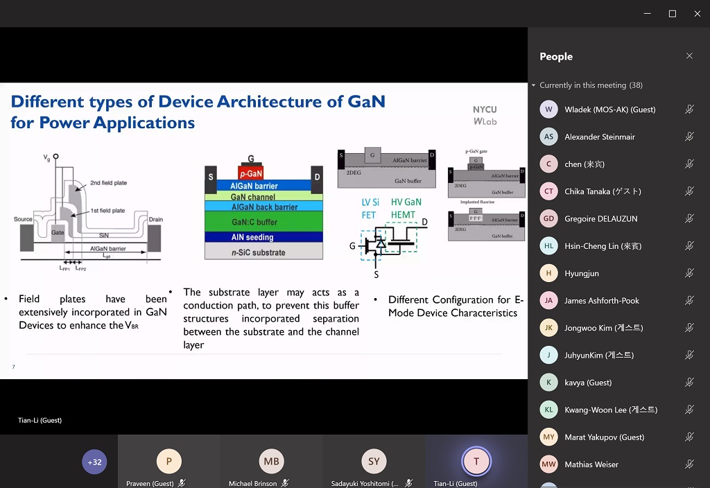
14:00 – 17:30 Benoit Bakeroot (Ghent University, Belgium), “GaN semiconductor devices for power electronics: overview, status and future perspectives”

23 September 2021

09.00 – 12:30 Qiang Li (UETSC, China), “Subthreshold and near-threshold ADC techniques”

14:00 – 17:30 Andrea Mazzanti (University of Pavia, Italy) and Enrico Monaco (Inphi, Italy), “Introduction and advances in serial links”

John von #Neumann: From the #Manhattan Project to the #Princeton Architecture https://t.co/xU9zjC15C2 #semi https://t.co/aX4ApJr5Ch


from Twitter https://twitter.com/wladek60

February 28, 2021 at 05:34PM
via IFTTT

Feb 27, 2021

Feb 26, 2021

[DAY 2] 1st Asia/South Pacific MOS-AK Workshop

Arbeitskreis Modellierung von Systemen und Parameterextraktion
Modeling of Systems and Parameter Extraction Working Group
1st Asia/South Pacific MOS-AK Workshop
(virtual/online) FEB. 25-26, 2021

Day2: FEB.26
Session C Chair: Sadayuki Yoshitomi, Kioxia (J)

[8] eSim: An open source CAD software for circuit simulation
Kannan Moudgalya
IIT Bombay (IN)

[9] A modular approach to next generation Qucs
Felix Salfelder and Mike Brinson
QUCS Team; Centre for Communications Technology, London Metropolitan University (UK)

[12] Machine learning-based approach to model and analyze GaN power devices
Tian-Li Wu
National Yang Ming Chiao Tung University, Taiwan (TW)

[11] TCAD-inspired compact modeling approach
Sung-Min Hong and Kwang-Woon Lee
Gwangju GIST (KR)

Session D Chair: Sheikh Aamir Ahsan, NIT Srinagar (IN)
[10] An Innovative Technique for Ultrafast Carrier Dynamics and THz Conductivities of Semiconductor Nanomaterials
Praveen Kr. Saxena and Fanish Kr. Gupta
Tech Next Lab, Lucknow (IN)

[13] Compact Modeling of 3D NAND Flash Memory for Diverse Unconventional Analog Applications
Shubham Sahay
IIT Kanpur (IN)

[14] Steep Subthreshold Slope PN-Body Tied SOI-FET for Ultralow Power LSI, Sensor, and Neuromorphic Chip
Takayuki Mori and Jiro Ida
Kanazawa Institute of Technology, Nonoichi (J)

[Pic] Group photo of selected MOS-AK participants attending 2nd Day of the workshop


[DAY 1] 1st Asia/South Pacific MOS-AK Workshop

Arbeitskreis Modellierung von Systemen und Parameterextraktion
Modeling of Systems and Parameter Extraction Working Group
1st Asia/South Pacific MOS-AK Workshop
(virtual/online) FEB. 25-26, 2021

DAY 1: FEB. 25, 2021
Session A Chair: Usha Gogineni, ams AG, Hyderabad (IN)

[1] New Insights in Low Frequency Noise Characteristics in PE-BJTs
Peijian Zhang and Ma Long
Science and Technology on Analog Integrated Circuit Laboratory; WHU (CN), Keysight Technologies (US)

[2] Direct white noise characterization of short-channel MOSFETs
K. Ohmori and S. Amakawa
DeviceLab, Tsukuba (J)

[3] SPICE Modeling of 2D-material based FETs with Schottky-barrier contacts
Sheikh Aamir Ahsan
Nanoelectronics Research and Development Group, NIT Srinagar, Jammu and Kashmir (IN)


[4] Physics-based model of SiC MOSFETs including high voltage and current regions
Sourabh Khandelwal, Cristino Salcines, and Ingmar Kallfass
Macquarie University Sydney (AU), University of Stuttgart (D)

Session B Chair: Daniel Tomaszewski, IMiF, Warszaw (PL)
[5] Compact Modeling for Gate-All-Around FET Technology
Avirup Dasgupta
IIT Roorkee (IN)


[6] BSIM-HV: Advanced High Voltage MOSFET Compact Model
Harshit Agarwal
IIT Jodhpur (IN)

[7] ASCENT+ Transnational Access for the nanoelectronics
Georgios Fagas
Tyndall (IE)

[Pic] Group photo of selected MOS-AK participants attending 1st Day of the workshop

[https://t.co/42ahdl8o1h] Study Captures #India's Rise in #Nanoelectronics Research https://t.co/xGqsmBiKKa #semi https://t.co/XNnB7RP3Fn


from Twitter https://twitter.com/wladek60

February 26, 2021 at 02:32PM
via IFTTT

President Biden signed an executive order Wednesday addressing growing concern over a global semiconductor shortage hampering the production of goods like automobiles and smartphones. https://t.co/JGZVSGVeSF #semi https://t.co/vWAg7EaYW8


from Twitter https://twitter.com/wladek60

February 26, 2021 at 02:16PM
via IFTTT

Feb 25, 2021

[Infineon Technologies] #quantum #computing development


from Twitter https://twitter.com/wladek60

February 24, 2021 at 11:46PM
via IFTTT

Feb 23, 2021

[papers] Compact/SPICE Modeling

[1] Wang, Jie; Chen, Zhanfei; You, Shuzhen; Bakeroot, Benoit; Liu, Jun; Decoutere, Stefaan; "Surface-Potential-Based Compact Modeling of p-GaN Gate HEMTs" Micromachines (2021) 12, no. 2: 199; https://doi.org/10.3390/mi12020199

Abstract: We propose a surface potential (SP)-based compact model of p-GaN gate high electron mobility transistors (HEMTs) which solves the Poisson equation. The model includes all possible charges in the GaN channel layer, including the unintended Mg doping density caused by out-diffusion. The SP equation and its analytical approximate solution provide a high degree of accuracy for the SP calculation, from which the closed-form I–V equations are derived. The proposed model uses physical parameters only and is implemented in Verilog-A code.

Fig: The equivalent circuit of the capacitance of field plates (FPs) of a p-GaN gate HEMT.


[2] Chen, H. and He, L.,  The spatial and energy distribution of oxide trap responsible for 1/f noise in 4H-SiC MOSFETs. Journal of Physics Communications, JPCO-101816.R1 (2021)

Abstract: Low-frequency noise is one of the important characteristics of 4H-SiC metal-oxide-semiconductor field-effect transistors (MOSFETs) that is susceptible to oxide traps. Drain-source voltage noise models of 4H-SiC MOSFETs under low–drain-voltage and inverse condition were proposed by considering the spatial and energy non-uniform distribution of the oxide trap, based on the McWhoter model for uniform trap distribution. This study performed noise experiments on commercial 4H-SiC MOSFETs, and revealed that the non-uniform spatial and non-uniform energy distribution caused new 1/f noise phenomenon, different from that under uniform spatial and energy distribution. By combining experimental data and theoretical models, the spatial and energy distribution of oxide traps of these samples were determined.
Fig: Adaptive circuit for 4H-SiC MOSFET noise measurement
in the frequency 1 Hz-10kHz ranged


Feb 22, 2021

[Kioxia] Less is more: the challenge of #3D-#NAND memory https://t.co/N5eEZAOL16 #semi https://t.co/Tm7fNXTynD


from Twitter https://twitter.com/wladek60

February 22, 2021 at 06:24PM
via IFTTT

#TSMC vs #Intel https://t.co/kNtoOcTRFx #semi @mannerisms @semiwiki https://t.co/eMLyKrFdY1


from Twitter https://twitter.com/wladek60

February 22, 2021 at 02:49PM
via IFTTT

[https://t.co/FrgrQhA6mP] #India needs chipset manufacturers — lots of them. Here is why. https://t.co/VrJw27rpFp #semi https://t.co/nq0KKtrJVP


from Twitter https://twitter.com/wladek60

February 22, 2021 at 02:07PM
via IFTTT

[3D Printing Industry] Researchers open up low-cost #opensource #microfluidics #3D printing - https://t.co/VwPoWIzI72 #semi https://t.co/OyfmccoCb9


from Twitter https://twitter.com/wladek60

February 22, 2021 at 02:04PM
via IFTTT

Feb 19, 2021

Virtual Si Museum /2107/ TG4 and TG50

The TG1-TG5 series transistor are the first industrially mass-produced BJT transistors in Poland. The serial production was started by the TEWA Semiconductor Factory, Warsaw, in early1960s. Then, the TG50-TG55 series, was also manufactured by the TEWA in 1961–1962. 

The TG4 (see Pic: below) is low power, low frequency, pnp germanium (Ge) alloy transistor (with 75 mW max collector power) [1].

The TG50 (below) is medium power, low frequency,  pnp germanium (Ge) alloy transistor (with 175 mW max collector power) [2].

An initial stage of Polish semiconductor microelectronics research activities has been reviewed by Prof. Jerzy Pułtorak. In his paper [3], he has reviewed activities of leading Polish R&D groups starting from Department of Electronics, Polish Academy of Sciences (PAN) founded on July 4, 1952 till foundation of the Instytut Technologii Elektronowej (ITE, Warsaw) early 1960 (now Sieć Badawcza Łukasiewicz - Instytut Mikroelektroniki i Fotoniki).  The first, in Poland, experimental germanium point-contact transistor TP-1 [4] has been developed by Prof. Rosinski just after John Bardeen, Walter Brattain and William Shockley have invented a semi-conductor triode (transistor) [5] on December 23, 1947.

Pic: TG4 and two TG50 by the TEWA Semiconductor Factory, Warsaw (PL)

References: 
[1] TG1-5 / PL Wikipedia/ https://pl.wikipedia.org/wiki/TG1-5
[2] TG50-5  / PL Wikipedia/ https://pl.wikipedia.org/wiki/TG50-55
[3] J. Pułtorak, "60 years of polish transistors," 2014 Proceedings of the 21st International Conference Mixed Design of Integrated Circuits and Systems (MIXDES), Lublin, Poland, 2014, pp. 15-21, doi: 10.1109/MIXDES.2014.6872144.
[4] W.Rosinski, J.Groszkowski, “Doswiadczalne tranzystory punktowe model TP” (“Experimental point-cotact transistors model TP”), Arch. Elektrot. 4, 1955, p. 381
[5] J.Bardeen, H.W.Brattain, “The transistor, a semi-conductor triode”, Phys.Rev.74, 7, 1954, p.230


Feb 18, 2021

#Linux Foundation, #DARPA collaborate on #opensource for #5G https://t.co/AHyNjyTjHJ #semi https://t.co/2BrfkspWSl


from Twitter https://twitter.com/wladek60

February 18, 2021 at 09:02PM
via IFTTT

[mos-ak] [Final Program] 1st Asia/South Pacific MOS-AK Workshop (Online) FEB. 25-26, 2021


Together with IEEE Young Professionals (at iitk.ac.in), the MOS-AK workshop online host as well as all the Extended MOS-AK TPC Committee, we have the pleasure to invite to the very first Asia/South Pacific MOS-AK Workshop which will be Virtual/Online event. Scheduled, 1st Asia/South Pacific MOS-AK Workshop, aims to strengthen a network and discussion forum among experts in the field, enhance open platform for information exchange related to compact/SPICE modeling and Verilog-A standardization, bring people in the compact modeling field together, as well as obtain feedback from technology developers, circuit designers, and TCAD/EDA tool developers and vendors.

The MOS-AK workshop program is available online

Venue: Virtual/Online MOS-AK Workshop - FEB. 25-26, 2021
  • Day 1 (FEB.25) begins: 8:00 in Europe; 12:30 in India; 15:00 in China
  • Day 2 (FEB.26) begins: 8:00 in Europe; 12:30 in India;15:00 in China
Registered participant will receive online meeting invitation
(any related enquiries can be sent to register@mos-ak.org)

Postworkshop Publications: Selected best MOS-AK technical presentation will be recommended for further publication in a special Solid State Electronics (SSE) issue on compact modeling.

W.Grabinski on the behalf of International MOS-AK Committee
WG18022021

--
You received this message because you are subscribed to the Google Groups "mos-ak" group.
To unsubscribe from this group and stop receiving emails from it, send an email to mos-ak+unsubscribe@googlegroups.com.
To view this discussion on the web visit https://groups.google.com/d/msgid/mos-ak/CALp-Rj84YhCntEfry9%3DmQkeprAkB6cWtMcZ4RnFvVSNgh7pa7g%40mail.gmail.com.

[linux] Conferences and Events

Python Web Conf - March 22 - 26, 2021
The 3rd annual Python Web Conf is a virtual event designed to promote best practices for hard web production problems. It features international experts presenting on 48 topics such as Django, Flask, Pyramid, Tornado, Plone, CI/CD, Containers, Serverless, REST APIs, web security, microservices, websockets, etc.

DrupalCon - April 12 - 16, 2021
The open source digital experience conference for Drupal.

Black Hat Asia 2021 - May 4-7, 2021
During this week, information security experts will teach interactive, online Trainings, innovative research will be presented at Briefings, the latest open-source tools will be showcased at Arsenal, and the Business Hall will feature top-tier security solutions and service providers, plus ample networking events and opportunities.

Feb 17, 2021

#SIA has sent a letter to President Biden


from Twitter https://twitter.com/wladek60

February 17, 2021 at 03:39PM
via IFTTT

Top #banks join #Linux and #opensource patent #protection group https://t.co/5d9B4a3ysh #semi https://t.co/XKGg4ioc9p


from Twitter https://twitter.com/wladek60

February 17, 2021 at 03:21PM
via IFTTT

[Semiconductor Engineering by B.Moyer] #3D #FTJ stack for use in in-memory computing [Source: #IEDM/#Kioxia] https://t.co/oeNFCdXZTj #semi https://t.co/koAXAIKK03


from Twitter https://twitter.com/wladek60

February 17, 2021 at 09:22AM
via IFTTT

[s3.i-micronews] NVIDIA Tesla P100 GPU with HBM2 2.5D & 3D Packaging https://t.co/1vs2c4qtvA #semi https://t.co/Z7vaqr8GGr


from Twitter https://twitter.com/wladek60

February 17, 2021 at 09:14AM
via IFTTT

[papers] Compact/SPICE Modeling

[1] Peled, A, Amrani, O, Rosenwaks, Y.; DC and transient models of the MSET device; Int J Numer Model. 2021;e2869. https://doi.org/10.1002/jnm.2869
Abstract: As a multigate device, the multiple‐state electrostatically formed nanowire transistor (MSET) exhibits a rather complex characteristic on account of the coupling between each of its two adjacent terminals. The MSET has shown promise across a steadily growing range of applications and integrated circuit components. However, an analytical model of the MSET has not been formulated. The objective of this work was to develop practical DC and transient models of the MSET. The modeling approach comprises two stages: the first stage consists of a bottom‐up derivation of the I–V characteristics from the fundamental physical level using the physical processes within the device to derive equations that describe its steady‐state behavior; the second stage proposes a set of analytical equations more applicable to simulation environments. A transient model that considers device parasitic capacitance is also established. The models are validated against robust model simulations in TCAD Sentaurus and Cadence Virtuoso.

[2] Ciou, Jhang-Yan, Sourav De, Wallace Lin, Yao-Jen Lee, and Darsen Lu. "Analytical Modelling of Ferroelectricity Instigated Enhanced Electrostatic Control in Short-Channel FinFETs." arXiv e-prints (2020): arXiv-2007.
Abstract: This study simulated negative-capacitance double gate FinFETs with channel lengths ranging from 25nm to 100nm using TCAD. The results show that negative capacitance significantly reduces subthreshold swing as well as drain induced barrier lowering effects. The improvement is found to be significantly more prominent for short channel devices than long ones, which demonstrates the tremendous advantage of negative capacitance gate stack for scaled MOSFETs. A compact analytical formulation is developed to quantify sub-threshold swing improvement for short channel devices.
Fig: (a) Three-dimensional NC FinFET structure studied insimulation. (b) List of nominal device parameters used in TCAD simulation.

[3] Ahmed, Sheikh Z., Samiran Ganguly, Yuan Yuan, Jiyuan Zheng, Yaohua Tan, Joe C. Campbell, and Avik W. Ghosh. "A Physics Based Multiscale Compact Model of pin Avalanche Photodiodes." arXiv preprint arXiv:2102.04647 (2021).
Abstract: III-V material based digital alloy Avalanche Photodiodes (APDs) have recently been found to exhibit low noise similar to Silicon APDs. The III-V materials can be chosen to operate at any wavelength in the infrared spectrum. In this work, we present a physics-based SPICE compatible compact model for APDs built from parameters extracted from an Environment-Dependent Tight Binding (EDTB) model calibrated to ab-initio Density Functional Theory (DFT) and Monte Carlo (MC) methods. Using this approach, we can accurately capture the physical characteristics of these APDs in integrated photonics circuit simulations.
Fig: Schematic diagram of avalanche photodiode model and testbench used in the SPICE simulations.


#Fab For Europe


from Twitter https://twitter.com/wladek60

February 17, 2021 at 12:32AM
via IFTTT

Feb 15, 2021

First #opensource smartphone #ophthalmoscope: oDocs sets world record https://t.co/qcGFsogcyc #semi https://t.co/E8sj2P4req


from Twitter https://twitter.com/wladek60

February 15, 2021 at 09:44AM
via IFTTT

[book] Moore's Law: The Untold Story

Daniel Foty 
Moore's Law: The Untold Story 
CreateSpace Independent Publishing Platform 
August 18, 2017; pp. 400; ISBN: 978-1974698431 
 
“Moore's Law' has entered popular parlance in a variety of ways. But what exactly is "Moore‘s Law?" And how did it happen?
In this book. Daniel Foty - a PhD. engineer and commercial-grade veteran of more than twenty-f‌ive years in the semiconductor industry and allied f‌ields - takes the reader through the tangled and bizarre sequence of events that eventually led to ‘Moore’s Law” and the ubiquitous silicon technology which has resulted. The deep roots of this remarkable story go back some twenty centuries, and that story involves an unlikely collection of happenstances. Gifts of nature, and totally unexpected developments. Along the way, the reader meets many of the players in that story - from the well-known (such as Benjamin Franklin and Gordon Moore) to the (unfortunately) less—well-known (such as Jack Kilby and Robert Noyce). In the f‌inal analysis, “Moore's Law" was neither imposed nor discovered - but instead represents a remarkable concatenation of a series of natural flukes that compounded into a juggernaut. 
Written for the non-specialist, the untold story of “Moore's Law" is told here with fresh depth and proper historical insight.


Feb 12, 2021

[paper] ACM) Model in VHDL-AMS

A. S. Kumar, Ch. Rekha, Y. D. S. Raju 
Behavioral Modeling of the Advanced Compact MOSFET (ACM) Model with VHDL-AMS 
OAIJSE, Vol. 6, Issue 1, January 2021 
ISSN (Online) 2456-3293 

*Holymary Institute Of Technology And Science, Bogaram(V), Keesara (M), Hyderabad

Abstract: This paper reports a VHDL-AMS implementation of the Advanced Compact MOSFET (ACM) model. This behavioral model aims at being a reference model for ACM code developers, helping to implement and maintain simulators specic code. Simulation results from classical testbenches are presented and con_rm the correctness of the proposed model.
Fig: The used methodology propose this testbench [ref]

[ref] A. L. T. B. da Fonseca and F. R. de Sousa, "Behavioral modeling of the Advanced Compact MOSFET (ACM) model with VHDL-AMS," 2008 Joint 6th International IEEE Northeast Workshop on Circuits and Systems and TAISA Conference, Montreal, QC, 2008, pp. 169-172
doi: 10.1109/NEWCAS.2008.4606348.

Abstract: This paper reports a VHDL-AMS implementation of the Advanced Compact MOSFET (ACM) model. This behavioral model aims at being a reference model for ACM code developers, helping to implement and maintain simulators specific code. Simulation results from classical testbenches are presented and confirm the correctness of the proposed model.

Feb 11, 2021

[symposium] ISDCS 2021 Hiroshima University

ISDCS 2021
3-5, March 2021
Hiroshima University, Higashi-Hiroshima, Japan

The ISDCS is a premium international forum for scholars, scientists, educators, students and engineers to exchange their latest findings and technological advances in the field of devices, circuits and systems.

Keynote Speakers
  • Prof. Parthasarathi Chakrabarti, Director, IIEST Shibpur and Department of Electronics Engineering, IIT(BHU), India
    "Advanced Materials and Methods for Fabrication of Thin-film Transistor (TFT)-based Sensors"
  • Prof. Shinji Kaneko, Hiroshima University, Japan
    "SDGs Initiatives at Hiroshima University: Integrating Global Strategy and Regional Vitalization"
Invited Speakers
  • Prof. Sanatan Chattopadhyay, University of Calcutta, India
    "Voltage Assisted Quantum Dot Based MOS Devices for Electronic and Optoelectronic Applications"
  • Prof. Partha Bhattacharya, IIEST Shibpur, India
    "Performance Improvement of Graphene Derivative based Gas sensors: Role of Functional Group Tuning and Ternary Junction Formation"
  • Prof. Hafizur Rahaman, IIEST Shibpur, India
    "Tunnel Field Effect Transistors: Challenges and Opportunities"
  • Prof. Nillohit Mukherjee, IIEST Shibpur, India
    "Metal Oxide Semiconductors with Carbon Nanomaterials for Efficient Supercapacitive Type Energy Storage Devices"
  • Prof. Shigeyasu Uno, Ritsumeikan University, Japan
    "Electrochemical Impedance Sensor for Non-invasive Living Cell Monitoring toward CMOS Cell Culture Monitoring Platform"
  • Mr. Shigeru Shiratake, Corporate Vice President, DRAM, Emerging Memory Process Integration and Device Technology Micron Technology, Inc., USA
    "Challenges for DRAM scaling and performance enhancement"
  • Prof. Rihito Kuroda, Tohoku University, Japan
    TBD

Previous Conference:

[PhD Thesis] Chiara ROSSI; A novel approach for SPICE modeling of light and radiation effects in ICs; Présentée le 29 janvier 2021 à EPFL Lausanne pour l’obtention du grade de Docteur ès Sciences; DOI:10.5075/epfl-thesis-8422 https://t.co/nKSO7dyI1I #semi https://t.co/ruaQTavMH1


from Twitter https://twitter.com/wladek60

February 11, 2021 at 03:56PM
via IFTTT

[thesis] SPICE modeling of light and radiation effects in ICs

A novel approach for SPICE modeling of light and radiation effects in ICs
Chiara ROSSI
Présentée le 29 janvier 2021
à la Faculté des sciences et techniques de l’ingénieur Groupe de scientifiques IEL
Programme doctoral en microsystèmes et microélectronique
pour l’obtention du grade de Docteur ès Sciences
DOI:10.5075/epfl-thesis-8422

Modeling the interaction of ionizing radiation, either light or ions, in integrated circuits is essential for the development and optimization of optoelectronic devices and of radiation-tolerant circuits. Whereas for optical sensors photogenerated carriers play an essential role, high energy ionizing particles can be a severe issue for circuits, as they create high density of excess carriers in ICs substrate, causing parasitic signals. In particular, recent advances in CMOS scaling have made circuits more sensitive to errors and dysfunctions caused by radiation-induced currents, even at the ground level. TCAD simulations of excess carriers generated by light or radiation are not dedicated to large scale circuit simulations since only few devices can be simulated at a time and computation times are too long. Conversely, SPICE simulations are faster, but their accuracy is strictly dependent on the correctness of the compact models used to describe the devices, especially when dealing with photocurrents and parasitic radiation-induced currents.
The objective of this thesis is to develop a novel modeling approach for SPICE compatible simulations of electron-hole pairs generated by light and by high energy particles. The approach proposed in this work is based on the Generalized Lumped Devices, previously developed to simulate parasitic signals in High Voltage MOSFET ICs. Here, the model is extended to include excess carriers generation. The developed approach allows physics-based simulations of semiconductor structures, hit by light or radiation, that can be run in standard circuit simulators without the need for any empirical parameter, only relying on the technological and geometrical parameters of the structure, and without any predefined compact model. The model is based on a coarse mesh of the device to obtain an equivalent network of Generalized Lumped Devices. The latter predicts generation of excess carriers and their propagation, recombination and collection at circuit nodes through the definition of equivalent voltages, proportional to the excess carrier concentrations, and equivalent currents, proportional to the excess carrier gradients. The model is validated with commercial TCAD numerical simulations for different scenarios. Regarding light effects, the proposed strategy is applied to simulate various optoelectronic devices. Complete DC I-V characteristics of a solar cell and transient response of a photodiode are studied. Next, phototransistors are considered. After, a full pixel of a 3T-APS CMOS image sensor is analyzed. The photosensing device, described with Generalized Devices, is co-simulated with the in-pixel circuit, described with compact models. The impact of semiconductor parameters on pixel output and on crosstalk between adjacent pixels is predicted. Finally, radiation-induced soft errors in ICs are examined. Alpha particles at different energies hitting the substrate are simulated. Parasitic currents collected at contacts are studied as a function of particles position and energy. Funneling effect, which is a phenomenon specific to high injection, is also included in the model.
This work shows that the Generalized Lumped Devices approach can be successfully used for SPICE simulations of optoelectronic devices and for prediction of radiationinduced parasitic currents in ICs substrate. This thesis is a first step towards a complete and flexible tool for excess carriers modeling in standard circuit simulators.
Fig: Layout, mesh (gray dashed lines) and equivalent network of Generalized Lumped Devices (Generalized Homojunctions, Resistors and Diodes). The structure is uniformly illuminated from the left side, justifying a 1D discretization scheme.


Feb 10, 2021

[papers] Compact/SPICE Modeling

[1] Kotecha, Ramachandra M., Md Maksudul Hossain, Arman Rashid, Asif Emon, Yuzhi Zhang, and Homer Ei C. Alan Mantooth. "Compact Modeling of High-Voltage Gallium Nitride Power Semiconductor Devices for Advanced Power Electronics Design." IEEE Open Journal of Power Electronics (2021)

Fig: (a) Structure of field-plated GaN transistor (b) Equivalent sub-circuit topology


[2] Sengupta, Sarmista, and Soumya Pandit. "A Unified Model of Drain Current Local Variability due to Channel Length Fluctuation for an n-Channel EδDC MOS Transistor." (researchsquare.com 2021).
Fig: Schematic diagram of an Epitaxial δ doped n-channel MOS transistor used for design purpose and the graded retrograde approximation of the channel profile of EδDC transistor.


[3] Patil, C.V., Suma, M.S. Compact modeling of through silicon vias for thermal analysis in 3-D IC structures. Sādhanā 46, 35 (2021). https://doi.org/10.1007/s12046-020-01549-1
Fig: Through Silicon Via 2D representation and its equivalent subcircuit.


Feb 9, 2021

[TechCrunch] CHIPS Alliance hires new director to push #opensource #chips ecosystem into next gear https://t.co/hAWwzdXknn #semi https://t.co/xHgTbWv2kU


from Twitter https://twitter.com/wladek60

February 09, 2021 at 02:00PM
via IFTTT

[paper] On-Chip Coplanar Waveguides

José Valdés-Rayón, Roberto S. Murphy-Arteaga and Reydezel Torres-Torres; 
Determination of the Contribution of the Ground-Shield Losses 
to the Microwave Performance of On-Chip Coplanar Waveguides 
IEEE Transactions on MTT; Feb.3, 2021 
DOI: 10.1109/TMTT.2021.3053548 
* National Institute of Astrophysics, Optics and Electronics (INAOE), Department of Electronics, Tonantzintla, Puebla 72840, Mexico.

Abstract: In this article, we characterize and model two parasitic effects that become apparent in the performance of coplanar waveguide interconnects in CMOS. One is the transverse resistance introduced by a patterned ground shield in coplanar waveguide interconnects, which significantly contributes to the shunt losses. The other one is the parasitic coupling between the input and output ports through the ground shield. The latter effect is particularly accentuated in relatively short lines and complicates the determination of the propagation constant using line-line algorithms at several tens of gigahertz. We demonstrate that using the proposed methodology, excellent model-experiment correlation can be achieved in the modeling of these types of interconnects up to at least 60 GHz.

Funding: CONACyT-Mexico

#Fraunhofer Institutes kicks off #6G research project in #Germany https://t.co/djljw87w42 #semi https://t.co/noOrjd4Ikf


from Twitter https://twitter.com/wladek60

February 08, 2021 at 11:34PM
via IFTTT

Feb 8, 2021

Researchers review advancements in the development of #stretchable #transistors https://t.co/kQmvJGyMy4 #semi https://t.co/7sVc9uHZCR


from Twitter https://twitter.com/wladek60

February 08, 2021 at 06:36PM
via IFTTT

[C4P] MIXDES 2021 Paper Submission Deadline: 15 March 2021


MIXDES 2021 regular paper submission deadline is upcoming . As current COVID pandemic situation is still uncertain, the conference will be organized in hybrid mode or fully online. To help you with preparation of excellent papers, we have decided to move the submission deadline to 15 March 2021. As in previous year we are going to give you an opportunity to publish extended versions of your conference papers in Energies Journal. The information about the postMIXDES publication will be provided soon at the conference site (www.mixdes.org).

Important dates:
Conference days: 24-26 June 2021
Paper submission deadline: 15 March 2021
Notification of acceptance: 26 April 2021
Final paper versions: 17 May 2021

Mariusz Orlikowski - MIXDES 2021 Conference Secretary


Thanks to @johndmcmaster, we're in business again for the CPS-A-01 (DL-0311) Ok hand #CPS1 #CPS2 https://t.co/JqPzNlOUBy #semi https://t.co/VUxxNz2vHS


from Twitter https://twitter.com/wladek60

February 08, 2021 at 03:41PM
via IFTTT

#Metamaterials’ potential for transforming #electronics https://t.co/uHlxv7C5M4 #semi https://t.co/6Yc9TxD82f


from Twitter https://twitter.com/wladek60

February 08, 2021 at 03:18PM
via IFTTT

[IEEE Spectrum] New Type of #DRAM Could Accelerate #AI https://t.co/QWucai2xJX #semi https://t.co/KtNPpyw4Cj


from Twitter https://twitter.com/wladek60

February 08, 2021 at 02:58PM
via IFTTT

[paper] Simulations of transient processes in the nc-MOS structures

D. Tanous, A. Mazurak and B. Majkusiak 
Simulations of transient processes and characteristics of the nc-MOS structures 
Microelectronic Engineering, 
Volume 178, 2017, pp/ 173-177, 
DOI: 10.1016/j.mee.2017.05.013 

Abstract: Experimentally measured capacitance-voltage and current-voltage characteristics of the metal-insulator-semiconductor structures with nanocrystals embedded in the insulator often exhibit formations which result from charging/discharging processes of the nanocrystals and are difficult to explain and predict intuitively. Time dependent simulations as presented in this paper can be helpful in their analysis. The paper presents a study of the impact of selected geometrical parameters on their characteristics with the bias voltage ramp rate as a parameter.
FIG: a.) nc-MIS Structure; b.) Bias voltage ramp stimulation; c.)  CV and IV Simulations results

[C4P] 32nd IEEE MIEL 2021

32nd IEEE International Conference on Microelectronics 
MIEL 2021 
from September 12th-14th, 2021 in Niš, Serbia  

Due to the unprecedented health, travel and social distance restrictions imposed in Serbia and all over the world as a result of the COVID-19 pandemic, all participants will be invited to join a virtual MIEL 2021.

Accepted papers will be published in the Proceedings of the MIEL 2021 Conference, and included in IEEE Xplore database, subject to regular registration of at least one of the authors before July 16th, 2021. We are pleased to invite you, as an expert in the field of microelectronics, to submit paper to MIEL 2021 Conference and to encourage colleagues to do it. The deadline for the submission of two page-extended summaries (including figures, tables, and references) is May 7th, 2021. Looking forward to receiving your abstract for MIEL 2021 Conference

MIEL 2021 Program Committee
  • Vojkan Davidović
  • Danijel Danković

Feb 7, 2021

Feb 5, 2021

[Watchy by SQFMI] A fully open source & customizable E-Ink watch https://t.co/za6CFZIOr9 #semi https://t.co/VS1C92jwmV


from Twitter https://twitter.com/wladek60

February 05, 2021 at 11:46AM
via IFTTT

#IBM turns to #opensource software to build #quantum ecosystem https://t.co/FtYZ8sAY7A #semi https://t.co/ge7VMhfwR2


from Twitter https://twitter.com/wladek60

February 05, 2021 at 09:25AM
via IFTTT

Virtual Si Museum /2105/ IBM components from 1948 to 1986

Let's visit a partner's museum to discover IBM components from 1948 to 1986. Recently, Ken Shirriff /semiwiki.org/ has received a vintage display box used by IBM to illustrate the progress of computer technology. This display case, created by IBM Germany1 in 1986 included technologies ranging from vacuum tubes and magnetic core memory to IBM’s latest (at the time) memory chips and processor modules. In his semiwiki.org blog post, he describes these items in detail and how they fit into IBM’s history [read mode...]