Showing posts with label nanowire. Show all posts

Jul 19, 2023

[paper] artificial synapse

Md. Hasan Raza Ansari, Udaya Mohanan Kannan, and Nazek El-Atab
Silicon Nanowire Charge Trapping Memory for Energy-Efficient Neuromorphic Computing
IEEE Transactions on Nanotechnology (2023)
DOI 10.1109/TNANO.2023.3296673

SAMA Labs, CEMSE Division, KAUST, Thuwal 23955-6900, Saudi Arabia
Department of Electronic Engineering, Gachon University, Seongnam 13120, Korea

Abstract: This work highlights the utilization of the floating body effect and charge-trapping/de-trapping phenomenon of a Silicon-nanowire (Si-nanowire) charge-trapping memory for an artificial synapse of neuromorphic computing application. Charge trapping/de-trapping in the nitride layer characterizes the long-term potentiation (LTP)/depression (LTD). The accumulation of holes in the potential well achieves short-term potentiation (STP) and controls the transition from STP to LTP. Also, the transition from STP to LTP is analyzed through gate length scaling and high-κ material (Al2O3) for blocking oxide. Furthermore, the conductance values of the device are utilized for system-level simulation. System-level hardware parameters of a convolutional neural network (CNN) for inference applications are evaluated and compared to a static random-access memory (SRAM) device and charge-trapping memory. The results confirm that the Si-nanowire transistor with better gate controllability has a high retention time for LTP states, consumes low power, and archives better accuracy (91.27%). These results make the device suitable for low-power neuromorphic applications.


FIG: Schematic representation of biological and Si-nanowire charge trapping memory as an artificial synapse

Jun 14, 2023

[paper] Vertical Junction-Less Nanowire FETs

C. Maneux (University of Bordeaux), C. Mukherjee (CNRS), M. Deng (University of Bordeaux), G. Larrieu (CNRS), Y. WANG, B. Wesling, and H. Rezgui (University of Bordeaux)
Strategies for Characterization and Parameter Extraction of Vertical Junction-Less Nanowire FETs Dedicated to Design Technology Co-Optimization
H02-1863 (Invited) at 243rd ECS Meeting and SOFC-XVIII 
Boston, MA, May 29 - June 2, 2023

Abstract: In the era of emerging computing paradigms and artificial neural networks, hardware and functionality requirements are in the surge. In order to meet low power and latency criteria, new architectures for in-memory computing are being explored as alternatives to traditional von Neumann machines, which requires technological breakthrough at the semiconductor device level such as vertical gate-all-around junctionless nanowire field effect transistors (VNWFET), that can address many process challenges such as downscaling, short-channel effects, compactness and electrostatic control. Its integration in the mainstream design flow is not straightforward and requires design technology co-optimization (DTCO) at an early stage. This invited paper explores strategies for accurate characterization and parameter extraction of the VNWFETs to feed the DTCO compact models

Fig: Final verification using full 3D multiphysics device thermal simulation, accounting for both ballistic and diffusive heat flux

Apr 6, 2022

[paper] Compact Model of JLNGAA MOSFET in Verilog-A

Billel Smaani1,2, Shiromani Balmukund Rahi3 and Samir Labiod4
Analytical Compact Model of Nanowire Junctionless Gate-All-Around MOSFET
Implemented in Verilog-A for Circuit Simulation. 
Silicon (2022)
DOI: 10.1007/s12633-022-01847-9
   
1 Centre Universitaire Abdelhafid Boussouf, Mila, Algeria
2 Electronique Department, Constantine I University, Algeria
3 Department of Electrical Engineering, IIT Kanpur, India
4 Department of Physics, Skikda University, Algeria

Abstract: In the present research article, we have proposed an analytical compact model for Nanowire Junctionless Gate-All-Around (JLNGAA) MOSFET validated in all transistor’s operation regimes. The developed model having an analytical compact form of the current expressions, based on surface potential (ΦS), obtained from approximated solutions of Poisson’s equation. The proposed model has implemented in standard Verilog-A language using SMASH circuit simulator in order to be used in various commercial circuit simulators. The proposed model has also validated using ATLAS-TCAD simulation for various physical parameters such as the channel doping concentration (Nd) and the channel radius (R) of JLNGAA MOSFET. Finally, based on the developed Verilog-A JLNGAA MOSFET model, we have tested it in four types of low voltage circuits, CMOS inverter, CMOS NOR-Gate, an amplifier and a Colpitts oscillator.


Fig: Transient simulation of the implemented Colpitts oscillator using SMASH, where Vout is the output voltage. R = 4 nm, tox = 2 nm, L = 1 μm and Nd = 1E19/cm^3

Acknowledgments: Dr. S. B. Rahi (Indian Institute of Technology, Kanpur, India) for their useful suggestions

Jan 12, 2022

[paper] Compact Modelling of Si Nanowire/Nanosheet MOSFETs

A. Cerdeira1, M. Estrada1, and M. A. Pavanello2
On the compact modelling of Si nanowire and Si nanosheet MOSFETs
Semiconductor Science and Technology, vol. 37, no. 2, p. 025014, Jan. 2022.
DOI: 10.1088/1361-6641/ac45c0
   
1 Centro de lnvestigacién y de Estudios Avanzados del IPN, Mexico City, Mexico
2 Centro Universitario PEI, Sao Bernardo do Cainpo, Sao Paulo, Brazil


Abstract: In this paper, three-dimensional technology computer aided design simulations are used to show that the electron concentration, current density, and electric field distribution from the interface at the lateral channels and from the top channel to the centre of the silicon wire, in nanowire and nanosheet structures, are practically same. This characteristic makes it possible to consider that the total channel width for these structures is equal to the perimeter of the transistor sheet, allowing to extend of the application of the symmetric doped double-gate model (SDDGM) model to nanowires and nanosheets metal-oxide-semiconductor field effect transistors, with no need to include new parameters. The model SDDGM is validated for this application using several measured and simulated structures of nanowires and nanosheets transistors, with different aspect ratios of fin width and fin height, showing very good agreement between measured or simulated characteristics and modelled. SDDGM is encoded in Verilog-A language and implemented in SPICE circuit simulator.

Fig: a.) Normalized measured and modelled transfer characteristics of stacked transistor in the linear region at VDS=0.025V and in saturation region at VDS=0.75V; b.) Output characteristic and conductance at VGS=1V.

Acknowledgments: The authors are grateful to CEA—Leti for providing the exper- imental samples used in this paper. This work was supported by the CONACYT project 236887, CNPq, Sao Paulo Research Foundation (FAPESP) Grants 2015/ 1049 1-7 and 2019/ 15500- 5, and the IBM/STMicroelectronics/Leti Joint Development Alliance.


Dec 8, 2021

[paper] Analytical Compact Model Of Cylindrical Junctionless Nanowire FETs

Adelcio M. de Souza, Daniel R. Celino, Regiane Ragi, Murilo A. Romero
Fully analytical compact model for the Q–V and C–V characteristics 
of cylindrical junctionless nanowire FETs
Microelectronics Journal (2021): 105324
DOI: 10.1016/j.mejo.2021.105324
   
University of Sao Paulo (EESC/USP), Sao Carlos (BR)

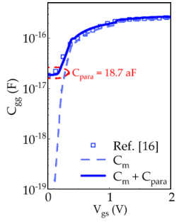
Abstract: This paper develops a new compact model for the Q–V and C–V characteristics of cylindrical junctionless nanowire FETs in which the nanowire radius is large enough, in such a way that quantum confinement effects can be neglected. Our model is fully analytical and valid for all bias regimes, i.e., subthreshold, partial depletion, and accumulation. The obtained Q-V and C–V characteristics, as well as their derivatives, are continuous across the full range of bias voltages. The model is fully physics-based, with no fitting parameters, and it is very intuitive, since it relies on the understanding of the device as a gated resistor. Model validation is performed against previous results in the literature, demonstrating very good agreement.
Fig.  Validation of our C–V model (solid lines) in comparison to numerical results, highlighting the effect of parasitic capacitance. The free-carrier capacitance component from new model is shown in dashed lines. Simulation parameters: tox = 4.5nm, Nd = 1.6E18 cm−3, L = 200nm, VFB = 1.09V and Vds = 0.05V.

Acknowledgments: The authors would like to thank the Brazilian funding agencies CAPES, CNPq, and Fapesp for their financial support: Conselho Nacional de Desenvolvimento Científico e Tecnologico. Grant Number: 303708/2017-4; Coordenaçao de Aperfeiçoamento de Pessoal de Nível Superior; Fundaçao de Amparo a Pesquisa do Estado de Sao Paulo. Grant Number: 18/13537-6.

Nov 9, 2021

8th EuroSOI-ULIS 2022 at University of Udine (Italy)

Organized by:
University of Udine (Italy)

Conference chair:
Pierpaolo Palestri

Local organizing Committee:
Francesco Driussi
David Esseni
Daniel Lizzit

Conference Secretariat:
Centro Congressi Internazionali 

Steering Committee:
  • Francis BALESTRA
    (IMEP Minatec, France)
  • Maryline BAWEDIN
    (IMEP-LAHC, France)
  • Cor CLAEYS
    (KU-Leuven, Belgium)
  • Bogdan CRETU
    (ENSICAEN, France)
  • Sorin CRISTOLOVEANU
    (IMEP-LAHC, France)
  • Francisco GAMIZ
    (UnivGranada, Spain)
  • Elena GNANI
    (Univ. of Bologna, Italy)
  • Benjamin INIGUEZ 
    (URV, Spain)
  • Joris LACORD
    (CEA-Leti, France)
  • Enrico SANGIORGI
    (Univ.Bologna, Italy)
  • Luca SELMI
    (Univ. of Modena, Italy)
  • Viktor SVERDLOV
    (TU Wien, Austria)
  • Andrei VLADIMIRESCU
    (ISEP, France)
Sponsors:


8th Joint International EuroSOI Workshop and International Conference
on Ultimate Integration on Silicon (EuroSOI-ULIS) 2022
May 18-20, 2022 – Udine, Italy

https://eurosoiulis2022.com

The Conference aims at gathering together scientists and engineers working in academia, research centers and industry in the field of SOI technology and nanoscale devices in More-Moore and More-Than-Moore scenarios. High quality contributions in the following areas are solicited:
  • Advanced SOI materials and structures, innovative SOI-like devices.
  • Alternative transistor architectures (FDSOI, Nanowire, FinFET, MuGFET, vertical MOSFET, FeFET and TFET, MEMS/NEMS, Beyond-CMOS).
  • New channel materials for CMOS (strained Si/Ge, III-V, carbon nanotubes; graphene and other 2D materials).
  • Properties of ultra-thin semiconductor films and buried oxides, defects, interface quality; thin gate dielectrics: high-κ and ferroelectric materials for switches and memory.
  • New functionalities and innovative devices in the More than Moore domain: nanoelectronic sensors, biosensor devices, energy harvesting devices, RF devices, imagers, integrated photonics (on SOI), etc.
  • Transport phenomena, compact modeling, device simulation, front- and back-end process simulation.
  • CMOS scaling perspectives; device/circuit level performance evaluation; switches and memory scaling; three-dimensional integration of devices and circuits, heterogeneous integration.
  • Advanced test structures and characterization techniques, parameter extraction, reliability and variability assessment techniques for new materials and novel devices.
Original 2-page abstracts with illustrations will be reviewed by the Scientific Committee. The accepted contributions will be published as 4-page letters in a special issue of the Elsevier journal Solid-State Electronics. Extended versions of outstanding papers will be published in a further special issue of Solid-State Electronics. A best poster award will be attributed by ELSEVIER. 

The “Androula Nassiopoulou Best Paper Award"
will be attributed by the SINANO institute.

Important dates:
  • abstract submission deadline: March 1, 2022
  • notification of acceptance: March 15, 2022

Oct 21, 2021

[paper] Charge-based Modeling of FETs

Jean-Michel Sallese 
Charge-based modeling of field effect transistors, Make it easy
Joint International EUROSOI and EuroSOI-ULIS Workshop (Sept.2020)
DOI: 10.1109/EuroSOI-ULIS53016.2021.956068
 
EDLab, EPFL,  Lausanne  (CH)
 
Abstract: In this presentation, we revisit some charge voltage dependencies for different architectures of field effect transistor, emphasizing on compactness and simplicity while maintaining a close link with physics, which makes these models predictive and accurate for general purposes of compact modeling.

Fig: The gm/I invariant versus the inversion coefficient IC. 
The operation modes of the MOSFET are clearly defined. 

Acknowledgements: I (JMS) would like to thank F. Jazaeri, C. Lallement, W. Grabinski, B. Iniguez and M. Bucher for their constructive interactions. 


May 26, 2021

[Review] Nanosheet Transistors Technology

Firas N. A. Hassan Agha1, Yasir H. Naif2, Mohammed N. Shakib3
Review of Nanosheet Transistors Technology
Tikrit Journal of Engineering Sciences (2021) 28 (1): 40-48
ISSN: 1813-162X (Print) ; 2312-7589 (Online)
DOI: http://doi.org/10.25 30/tjes.28.1.05
available online at: http://www.tj-es.com

1Electrical Department/ Engineering College; Mosul University; Mosul, Iraq
2Department of Computer Engineering; Faculty of Engineering, Tishk; International University; Erbil, Iraq
3Faculty of Electrical and Electronics; Engineering Technology, University; Malaysia Pahang; Pekan, Malaysia


Abstract: Nano-sheet transistor can be defined as a stacked horizontally gate surrounding the channel on all direction. This new structure is earning extremely attention from research to cope the restriction of current Fin Field Effect Transistor (FinFET) structure. To further understand the characteristics of nano-sheet transistors, this paper presents a review of this new nano-structure of Metal Oxide Semiconductor Field Effect Transistor (MOSFET), this new device that consists of a metal gate material. Lateral nano-sheet FET is now targeting for 3nm Complementary MOS (CMOS) technology node. In this review, the structure and characteristics of Nano-Sheet FET (NSFET), FinFET and NanoWire FET (NWFET) under 5nm technology node are presented and compared. According to the comparison, the NSFET shows to be more impregnable to mismatch in ON current than NWFET. Furthermore, as comparing with other nano-dimensional transistors, the NSFET has the superior control of gate all-around structures, also the NWFET realize lower mismatch in sub threshold slope (SS) and drain induced barrier lowering (DIBL).
Fig: Development of Field Effect Transistor from FinFET to MBCFET [Credit: Samsung]

Acknowledgment: The authors would like to thank University of Mosul for their support.


Nov 30, 2020

[paper] The advantages of p-GaN channel/Al2O3 gate insulator

Maria Ruzzarin,1, Carlo De Santi,1 Feng Yu,2 Muhammad Fahlesa Fatahilah,2 Klaas Strempel,2 Hutomo Suryo Wasisto,2 Andreas Waag,2 Gaudenzio Meneghesso,1 Enrico Zanoni,1
and Matteo Meneghini1
Highly stable threshold voltage in GaN nanowire FETs: The advantages of p-GaN channel/Al2O3 gate insulator
Appl. Phys. Lett. 117, 203501 (2020); 
DOI: 10.1063/5.0027922
Published Online: 16 November 2020

1 Department of Information Engineering, University of Padova, via Gradenigo 6/b, 35131 Padova, Italy
2 Institute of Semiconductor Technology (IHT) and Laboratory for Emerging Nanometrology (LENA), Technische Universitat Braunschweig, Langer Kamp 6a/b, 38106 Braunschweig, Germany


Abstract: We present an extensive investigation of the charge-trapping processes in vertical GaN nanowire FETs with a gate-all-around structure. Two sets of devices were investigated: Gen1 samples have unipolar (n-type) epitaxy, whereas Gen2 samples have a p-doped channel and an n-p-n gate stack. From experimental results, we demonstrate the superior performance of the transistor structure with a p-GaN channel/Al2O3 gate insulator in terms of dc performance. In addition, we demonstrate that Gen2 devices have highly stable threshold voltage, thus representing ideal devices for power electronic applications. Insight into the trapping processes in the two generations of devices was obtained by modeling the threshold voltage variations via differential rate equations.

Fig. a) The p-channel device (Gen2) comprises a 2.5 lm n-GaN buffer layer, a 0.5 lm p-GaN channel layer, 0.73 lm n-GaN and 0.5 lm n p-GaN as the top layer, and 25 nm-Al2O3 as the gate dielectric.
b) SEM images of a nanowire of the p-channel device (Gen2) and bird’s-eye view of vertically aligned n-p-n GaN nanowire (NW) arrays with top contacts.

Aknowledgement: This work was supported in part by NoveGaN (Univ. of Padova) through the STARS CoG Grants call. Ack prog. Eccellenza. This research was partly performed within project INTERNET OF THINGS: SVILUPPI METODOLOGICI, TECNOLOGICI E APPLICATIVI and co-funded (2018–2022) by the Italian Ministry of Education, Universities and Research (MIUR) under the aegis of the “Fondo per il finanziamento dei dipartimenti universitari di eccellenza” initiative (Law 232/2016). Financial support from the German Research Foundation (DFG) of 3D GaN project and the Lower Saxony Ministry of Science and Culture (N-MWK) of LENA-OptoSense group is highly acknowledged for the development of vertical GaN nanowire FETs.

Jul 29, 2020

[paper] Vertical III-V Nanowire MOSFETs on Si

Olli-Pekka Kilpi, Markus Hellenbrand, Johannes Svensson, Axel R. Persson, Reine Wallenberg, Erik Lind, Member, IEEE, and Lars-Erik Wernersson
High-Performance Vertical III-V Nanowire MOSFETs on Si With gm > 3 mS/μm
in IEEE EDL vol. 41, no. 8, pp. 1161-1164, Aug. 2020
DOI: 10.1109/LED.2020.3004716

Abstract: Vertical III-V nanowire MOSFETs have demonstrated excellent performance including high transconductance and high Ion. One main bottleneck for the vertical MOSFETs is the large access resistance arising from the contacts and ungated regions. We demonstrate a process to reduce the access resistance by combining a gate-last process with ALD gate-metal deposition. The devices demonstrate fully scalable gm down to Lg = 25 nm. These vertical core/shell InAs/InGaAs MOSFETs demonstrate gm = 3.1 mS/μm and Ron = 190 μm. This is the highest gm demonstrated on Si. Transmission line measurement verifies a low contact resistance with RC = 115 μm, demonstrating that most of the MOSFET access resistance is located in the contact regions.
FIG: (a) of the MOSFET structure demonstrating benefit of the TiN gate metal;
(b )output characteristics of the vertical nanowire MOSFET 
with 90 nanowires, LG = 25 nm and diameter 17 nm.

Acknowledgment: This work was supported in part by the Swedish Research Council, in part by the Knut and Alice Wallenberg Foundation, in part by the Swedish Foundation for Strategic Research, and in part by the European Union H2020 Program INSIGHT under Grant 688784.

Jun 25, 2020

Neurotransistor MatLab Code

Eunhye Baek, Nikhil Ranjan Das, Carlo Vittorio Cannistraci, Taiuk Rim, Gilbert Santiago Cañón Bermúdez, Khrystyna Nych, Hyeonsu Cho, Kihyun Kim, Chang-Ki Baek, Denys Makarov, Ronald Tetzlaff, Leon Chua, Larysa Baraban and Gianaurelio Cuniberti
Intrinsic plasticity of silicon nanowire neurotransistors for dynamic memory and learning functions
Nat Electron (2020). 
DOI: 10.1038/s41928-020-0412-1

Abstract: Neuromorphic architectures merge learning and memory functions within a single unit cell and in a neuron-like fashion. Research in the field has been mainly focused on the plasticity of artificial synapses. However, the intrinsic plasticity of the neuronal membrane is also important in the implementation of neuromorphic information processing. Here we report a neurotransistor made from a silicon nanowire transistor coated by an ion-doped sol–gel silicate film that can emulate the intrinsic plasticity of the neuronal membrane. The neurotransistors are manufactured using a conventional complementary metal–oxide–semiconductor process on an 8-inch (200 mm) silicon-on-insulator wafer. Mobile ions allow the film to act as a pseudo-gate that generates memory and allows the neurotransistor to display plasticity. We show that multiple pulsed input signals of the neurotransistor are non-linearly processed by sigmoidal transformation into the output current, which resembles the functioning of a neuronal membrane. The output response is governed by the input signal history, which is stored as ionic states within the silicate film, and thereby provides the neurotransistor with learning capabilities.

FIG: Illustration of the structural similarity between the ion migration in the neurotransistor (left) and the membrane of a neuron cell in which the ionic current was modulated by a membrane potential (Vmemb) change in the case of the action potential (right)

Code availability: The MatLab code that supports the mathematical model in this article is available
at https://github.com/eunhye8747/MatLab-Code-Neurotransistor

Acknowledgements: This research was supported by the German Excellence Initiative via the Cluster of Excellence EXC1056 Center for Advancing Electronics Dresden (CfAED) and the MSIP (Ministry of Science, ICT and Future Planning), Korea, under the ICT Consilience Creative Program (IITP-R0346-16-1007) supervised by the IITP (Institute for Information & communications Technology Promotion). We acknowledge support from the Initiative and Networking Fund of the Helmholtz Association of German Research Centers through the International Helmholtz Research School for Nanoelectronic Networks (IHRS NANONET) (no. VH‐KO‐606) and German Research Foundation (DFG) via grants MA 5144/9-1, MA 5144/13-1 and MA 5144/14-1; BA4986/7−1, BA4986/8−1. Finally, we thank the INSA-DFG Bilateral Exchange Programme for financial support (IA/ DFG/2018/138, 12 April 2018). The authors thank S. Oswald (IFW Dresden) for the X-ray photoemission spectroscopy analysis of the ion-doped hybrid silicate films and M. Park (NamLab, Dresden) for the insightful discussion about the ionic polarization in the film. We thank R. Nigmetzianov (TU Dresden) for the film analysis.

Apr 24, 2013

TED Call for Papers on Compact Modeling of Emerging Devices

Compact Models (CMs) for circuit simulation have been at the heart of CAD tools for circuit design for almost five decades. As the mainstream CMOS technology is scaled into the nanometer regime, development of a truly physical and predictive CM for circuit simulation that covers geometry, bias, temperature, DC, AC, RF, and noise characteristics becomes a major challenge. The last call for a special issue on “advanced compact models and 45-nm modeling challenges” was in 2005. Seven years have passed, new technology nodes have been implemented, compact models have evolved and new compact models as well as compact models for new devices are being developed. Therefore, there is a need for another special issue dedicated to the advancement and challenges in core field-effect transistor (FET) models for 32-nm technologies and beyond as well as emerging technologies. For the core FET models, the associated noise/mismatch and reliability/variability models as well as proximity effects have become an essential part of the modeling effort. High-frequency, high-voltage, high-power, high-temperature devices have been extensively investigated, and their CMs are being reported in the literature. Device/circuit interaction and layout-dependent proximity effects are also hot topics today that are essential in nanometer chip designs. It is timely to report advances in these CMs in the 32-nm/22-nm technology era.

Concurrently, nonclassical MOSFETs as well as their CMs, such as multigate FinFETs and nanowire FETs, partially/fully-depleted ultrathin body (UTB) SOT, and thin-film transistors (TFTs), have emerged over the past decades. With the announcement of FinFETs being used in 22-nm and sub-22nm technology nodes, the need for such core models for fabless designers becomes an urgent reality. In these nonclassical devices, transistors are essentially short-channel, narrow-width, and thin-body. Tt is also an interesting topic to discuss and debate on the two different formalisms “top-down” drift-diffusion formulation adding ballistic effects versus “bottom-up” quasi-ballistic formulation adding scattering effects for modeling the real devices that are somewhere in between. Heterogeneous integration of various devices into the CMOS platform also becomes an important trend.
In addition, it is also timely to report advances in CMs of emerging devices beyond traditional silicon CMOS, such as different materials (III-V/Ge channel, organic) and different source/drain injection mechanisms (Schottky-barrier, tunneling, and junctionless FETs). These emerging device options for future VLSI building blocks have been studied extensively, while good physical CMs are still lacking. The special issue in these topics will stimulate research and development to promote modeling efforts such that theory would lead and guide technology realization and selection for future generations.
The special issue for the TRANSACTIONS ON ELECTRON DEVICES on compact modeling of emerging devices is devoted to the review and report of advancements in CMs for 32-nm technologies and beyond, including bulk and nonclassical CMOS and their associated noise/mismatch and reliability/variability models, as well as various emerging devices as future generation device options. It is timely as the industry is in the transition from traditional planar bulk-CMOS towards vertical FinFET technologies, and exploration of heterogeneous integration with various materials and structural choices.


Please submit manuscripts by using the following URL: http://mc.manuscriptcentral.com/ted
MAKE SURE TO MENTION THE SPECIAL ISSUE IN THE COVER LETTER

Paper submission Deadline: June 30, 2013
Scheduled Publication Date: February 2014

Guest Editors:
Xing Zhou, Nanyang Technological University, 
Jamal Deen, McMaster University, 
Benjamin Iniguez, Universitat Rovira i Virgili, 
Christian Enz, Swiss Federal Institute of Technology, 
Rafael Rios, Intel Corp.

If you have any questions about submitting a manuscript, please contact:
IEEE EDS Publications Office
445 Hoes Lane Piscataway JN 08854
Phone: +1 732 562 6855

Digital Object Identifier 10.1109/TED.2013.2253418