Nov 29, 2023

[mos-ak] [Final Program] 16th International MOS-AK Workshop Silicon Valley, Dec. 13, 2023

Arbeitskreis Modellierung von Systemen und Parameterextraktion 
Modeling of Systems and Parameter Extraction Working Group
16th International MOS-AK Workshop
Silicon Valley, December 13, 2023

Together with Keysight Technologies team, the MOS-AK workshop host as well as International MOS-AK Board of R&D Advisers and all the Extended MOS-AK TPC Committee, we have the pleasure to invite to consecutive, 16th International MOS-AK Workshop in Silicon Valley.

Scheduled 16th MOS-AK SPICE/Compact Modeling Workshop organized in the Silicon Valley, aims to strengthen a network and discussion forum among experts in the field, enhance open platform for information exchange related to compact/SPICE modeling and Verilog-A standardization, bring people in the compact modeling field together, as well as obtain feedback from technology developers, circuit designers, and TCAD/EDA tool developers and vendors. The content will be beneficial for anyone who needs to learn what is really behind the FOSS CAD/EDA IC simulation in modern device models in Open Access PDKs.

The MOS-AK workshop program is available online:

Venue:
Keysight Technologies
5301 Stevens Creek Boulevard
Santa Clara, CA 95051

Online Free Registration
any related enquiries can be sent to registration@mos-ak.org

-- W.Grabinski on the behalf of International MOS-AK Committee

WG291023

--
You received this message because you are subscribed to the Google Groups "mos-ak" group.
To unsubscribe from this group and stop receiving emails from it, send an email to mos-ak+unsubscribe@googlegroups.com.
To view this discussion on the web visit https://groups.google.com/d/msgid/mos-ak/CALp-Rj87GLh1GJ1VT6GZfqmYJO7bb1vyRvZ2M0uQgDZFaD8xng%40mail.gmail.com.

[paper] Noise modeling for cryogenic applications

Giovani Britton1,2, Salvador Mir2, Estelle Lauga-Larroze2, Benjamin Dormieu1, Quentin Berlingard3,4, Mickael Casse3 and Philippe Galy1
Noise modeling using look-up tables and DC measurements for cryogenic applications.
VLSI-SoC 2023 - 31st IFIP/IEEE International Conference on Very Large Scale Integration,
Oct 2023, Sharjah, United Arab Emirates.
DOI: 10.1109/VLSI-SoC57769.2023.10321896
hal-04305746
1STMicroelectronics, Crolles, France
2Univ. Grenoble Alpes, CNRS, Grenoble-INP, TIMA
3Univ. Grenoble Alpes, CEA, LETI
4Univ. Grenoble Alpes, CNRS, Grenoble-INP, IMEP-LAHC

Abstract : There is today a lack of mature transistor-level compact models for the simulation of integrated circuits at cryogenic temperatures. This is particularly the case for the simulation of the noise behavior which is critical for most applications. In this paper, we aim at an efficient prediction of the white noise behavior of basic amplifying stages working at RF frequencies and cryogenic temperatures. For this, we propose the use of DC measurements that are incorporated in a LookUp Table (LUT) and fed to a mathematical noise model. We illustrate the approach for the case of a transistor in common source configuration. The results of circuit simulation of the noise parameters in the standard temperature range are very close to the estimation of the same parameters using the LUT with just DC measurements. The approach can be readily extended to the analysis of circuits with multiple components. Next, the LUT approach is used for estimating the noise parameters at cryogenic conditions, considering DC measurements that have been carried out at these temperatures. The paper illustrates the feasibility of carrying out a cryogenic design using a LUT-based approach while accurate compact models are not yet available.

Fig : Measurement data and EKV or ACM generated parameters are added
to the LUT generated by the interface between EDA tools

Acknowledgments : This work was supported by the French program Conventions Industrielles de Formation par la Recherche (CIFRE) and Labex MINOS of French program ANR-10-LABX-55-01.

Nov 28, 2023

[PhD] ULTRARAM™ at Lancaster University

Lancaster University, Physics Department has three open PhD Projects, Programmes & Scholarships
  • Scaling ULTRARAM™ on FindAPhD.com
    The PhD project will further advance the development of ULTRARAM™ memory. ULTRARAM™ is an ultra-efficient, multi-award-winning memory technology that combines the non-volatility of flash with the speed and endurance of dynamic random access (DRAM).
  • Vertical-cavity surface-emitting lasers for below-screen consumer (and other) applications at Lancaster University on FindAPhD.com
    The PhD project will further develop a patented approach to implementing vertical-cavity surface-emitting lasers (VCSELs) operating at telecoms wavelengths
  • Novel compound-semiconductor logic for computing applications on FindAPhD.com
    The PhD project will further develop a patent-pending alternative approach to digital logic that abandons the CMOS paradigm underpinning computing
Supervisor: Prof. M. Hayne
Application deadline: 29 February 2024 // Competition Funded PhD Project (UK Students Only)

Nov 27, 2023

Chips JU Launch Event


https://www.chipsjulaunchevent.eu/

Agenda Day 1: Embracing the voice of stakeholders
12:00 - 14:30 Registration
13:00 - 15:30 Networking lunch and exhibition "Walk of Fame" opening and guided tour
15:30 - 15:40 Welcome and opening, Jari Kinaret, Executive Director of the Chips JU
15.40 - 16:00 Keynote speech, Thierry Breton, European Commissioner for Internal Market
16:00 - 16:20 Intro speeches "EU strategic autonomy and economic security"
  Nikolai Setzer, CEO, Continental AG
  Jaime Martorell, Special Commissioner for Microelectronics and Semiconductors, Spain
16:20 - 17:20 1st Panel discussion with a moderator
  Thomas Skordas, DDG, CNECT, European Commission
  Pierre Barnabé, CEO, Soitec
  Roger Dassen, CFO, ASML
  Luc Van den hove, President and CEO, imec
  Frédérique Le Grévès, President & CEO, STMicroelectronics France
  Cinzia Silvestri, CEO, Bi/ond
  Alain Jarre, Chairman and CEO, RECIF Technologies
17:20 - 17:40 Coffee break
17:40 - 18:00 Intro speeches "Maintaining and boosting European technology leadership"
  Jochen Hanebeck, CEO, Infineon Technologies AG
  Jo Brouns, Flemish Minister for Economy, Innovation, Work, Social Economy, and Agriculture
18:00 - 19:00 2nd Panel discussion with a moderator
  Signe Ratso, Deputy Director-General, DG RTD, European Commission
  European Semiconductor Board Member (name tbc)
  Stefan Finkbeiner, CEO, Bosch Sensortec GmbH
  Maurice Geraets, Executive Director, NXP Semiconductors Netherlands B.V.
  Sébastien Dauvé, CEO, CEA-Leti
  Eva Maydell, Member of the European Parliament
  Joost van Kuijk, CEO/CMO, Adimec
19:00 - 19:05 Closing remarks by the moderator
19:15 Shuttle bus to the social event venue
20:00 - 22:30 Social event and walking dinner “Art & History Museum of Belgium”

Day 2 Part 1: Presentation of the Initiative
08:00 - 09:00 Registration & welcome coffee
09:00 - 09:10 Intro speech by Lucilla Sioli, Director DG CNECT.A, European Commission
09:10 - 09:40 New advanced pilot lines:
Yves Gigase, Head of Programmes,
Anton Chichkov, Programme Officer, Chips JU
 
09:40 - 09:55 Network of competence centre: Yves Gigase, Head of Programmes, and Anton Chichkov, Programme Officer, Chips JU
09:55 - 10:10
  Cuting-edge quantum chips: Gustav Kalbe, acting Director DG CNECT C, and
  Christian Trefzger, Policy Officer, DG CNECT, European Commission
10:10 - 10:25 Chips Fund: EC, EIB, EIC joint presentation
10:25 - 10:55 Q&A
10:55 - 11:25 Coffee break, networking and exhibition
11:25 - 12:15 Interactive session on Advanced design platform:
Marco Ceccarelli and Matihew Xuereb, Policy Officers, DG CNECT, European Commission
12:15 - 13:40 Networking lunch.

Day 2 Part 2: Chips JU R&I Programme
13:40 - 13:50 Intro speech by Jean-Luc di Paola-Galloni,
Chair of the Chips JU Private Members Board
13:50 - 14:50 3rd Panel discussion with a moderator
  Lucilla Sioli, Director, DG CNECT.A, European Commission
  Michael Paulweber, Director Global ITS Research & Technology, AVL List
  Régis Hamelin, CTO, Blumorpho
  Francis Balestra, Director of Research CNRS
  Ferdinand Bell, Head of Public Collaborative Programs,
NXP Semiconductors, Germany GmbH
  Christoph Kutier, Vice-Chair, Fraunhofer Microelectronics Group/FMD
  Bert de Jonge, CEO, VERUM
14:50 - 15:20 ECS SRIA 2024 – What is new? Patrick Cogez, Technical Director, AENEAS IA
15:20 - 15:50 Upcoming Chips JU calls and focus topics
  Yves Gigase, Head of Programmes, and
Anton Chichkov, Programme Officer, Chips JU
15:50 - 16:00 Closing remarks
Jari Kinaret, Executive Director of the Chips JU
16:00 - 17:30 Coffee break, networking and exhibition

Nov 21, 2023

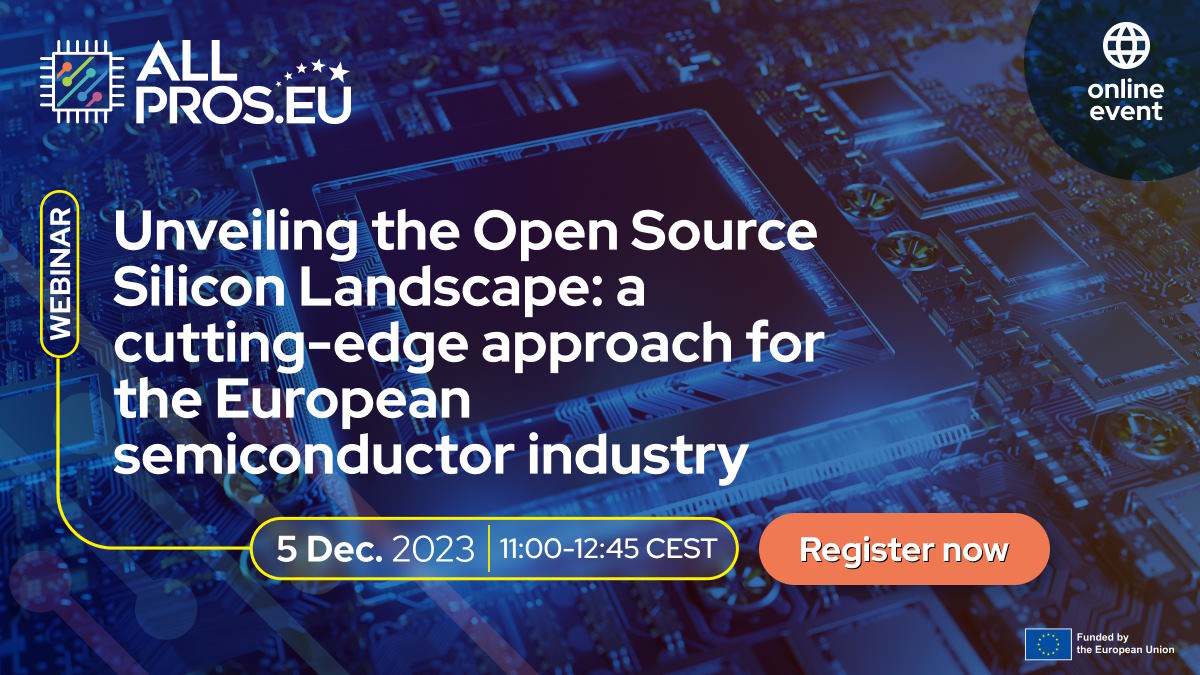
[webinar] Open Source Silicon Landscape

Unveiling the Open Source Silicon Landscape
a cutting-edge approach for the European semiconductor industry
5 December 2023


Who should attend and why:
  • Policymakers at the regional, national, and European level who want to strengthen their respective semiconductor ecosystem while collaborating and contributing to the Union’s industry as a whole
  • Research and academia representatives who are interested in deepening their knowledge or discovering the potential of the Open Source Silicon landscape
  • SMEs in the semiconductor industry who aim to expand and innovate their business by using a cutting-edge approach
  • Start-ups that are eager to elevate their business to the next level by embracing vanguard strategies
  • Citizen scientists and the general public who would like to have a better understanding of the new horizons in the semiconductor landscape
  • Experts active in industrial development who are interested in integrating potential new approaches
Registration:

The event is free of charge, but registration is mandatory. Registrants will receive the link to access the event by email.

Agenda:

11:00 - 11:05 Welcome
11:05 - 11:10 Introducing Open Source Silicon
11:10 - 11:20 BACKGROUND Open source silicon between software and hardware Background
11:20 - 11:40 POLICY BRIEF PRESENTATION Open source silicon’s position in the semiconductor value chain
11:40 - 12:35 PANEL Key opportunities and threats relevant to open source silicon strategies
12:35 - 12:45 Q&A and conclusions

Nov 20, 2023

[C4P] LAEDC 2024

CALL FOR PAPERS & POSTERS


LAEDC 2024 R&D topics of interest include, but are not limited to:
  • All electron-based devices
  • Electron Devices for Quantum Computing
  • RF-MMW-5G
  • Semiconductor-, MEMS- and Nanotechnologies
  • Packaging, 3D integration
  • Sensors and actuators
  • Display technology
  • Modeling and simulation
  • Reliability and yield
  • Device characterization
  • Reliability
  • Agrivoltaics

  • Flexible electronics
  • Biomedical Devices
  • Circuit-device interaction
  • Novel materials and process modules
  • Technology roadmaps
  • Electron device engineering education
  • Electron device outreach
  • Optoelectronics, photovoltaic and photonic devices and systems
  • Humanitarian Projects
  • STEM Initiatives
  • Energy harvesting
  • 2D Materials and Devices
IMPORTANT DATES:
  • Paper submission deadline: January 15, February 19, 2024
  • Author notification: April 1, 2024
  • LAEDC Conference Dates: MAY 8-10 2024
SPECIAL SESSIONS:
  • MOS-AK Workshop
  • IEEE EDS MQ
  • LAEDC Summer School
  • IEEE WIE/YP Session
  • Humanitarian Technology Session
ABOUT GUATEMALA:
Guatemala, country of Central America. The dominance of an Indigenous culture within its interior uplands distinguishes Guatemala from its Central American neighbours. The origin of the name Guatemala is Indigenous, but its derivation and meaning are undetermined. Some hold that the original form was Quauhtemallan (indicating an Aztec rather than a Mayan origin), meaning “land of trees,” and others hold that it is derived from Guhatezmalha, meaning “mountain of vomiting water” - referring no doubt to such volcanic eruptions as the one that destroyed Santiago de los Caballeros de Guatemala (now Antigua Guatemala), the first permanent Spanish capital of the region’s captaincy general. The country’s contemporary capital, Guatemala City, is a major metropolitan centre. Quetzaltenango, in the western highlands, is the nucleus of the Indigenous population.


Nov 16, 2023

Chipsalliance Technology Update - Nov. 2023

November 9, 2023

Check out the presentations below, and watch the replay here

  • Project Open Se Cura (slides)
    Kenny Vassigh, Bangfei Pan, Cindy Liu, Kai Yick, Google, Michael Gielda, Antmicro, Brian Murray, Verisilicon
  • Caliptra Workgroup Update (slides)
    Andres Lagar-Cavilla, Google
  • Enabling UVM testbenches in Verilator (slides)
    Michael Gielda, Karol Gugala, Antmicro
  • FuseSOC: Package manager and build abstraction tool for FPGA/ASIC development (slides)
    Olof Kindgren, Qamcom
  • CHIPYard: An Open Source RISC-V Design Framework (slides)
    Sagar Karandikar, U.C. Berkeley

Watch the Replay

Nov 14, 2023

[paper] Boropheneand Metal Interface

Vaishnavi Vishnubhotla, Sanchali Mitra, and Santanu Mahapatraa
First-principles based study of 8-Pmmn boropheneand metal interface
J. Appl. Phys. 134, 034301 (2023); doi: 10.1063/5.0144328
DOI 10.1063/5.0144328

Nano-Scale Device Research Laboratory, Department of Electronic Systems Engineering, 
Indian Institute of Science (IISc) Bangalore, India

Abstract: Borophene, the lightest member of mono-elemental 2D materials family, has attracted much attention due to its intriguing polymorphism. Among many polymorphs, digitally discovered 8-Pmmn stands out owing to its unique tilted-Dirac fermions. However, the property of interfaces between 8-Pmmn and metal substrates has so far remained unexplored, which has critical importance of its application in any electronic devices. Here, with the help of density functional theory, we show that the unique tilted-Dirac property is completely lost when 8-Pmmn borophene is interfaced with common electrode materials such as Au, Ag, and Ti. This is attributed to the high chemical reactivity of borophene as observed from crystal orbital Hamilton population and electron localization function analysis. In an effort to restore the Dirac property, we insert a graphene/hexagonal-boron-nitride (hBN) layer between 8-Pmmn and metal, a technique used in recent experiments for other 2D materials. We show that while the insertion of graphene successfully restores the Dirac nature for all three metals, hBN fails to do so while interfacing with Ti. The quantum chemical insights presented in this work may aid in to access the Dirac properties of 8-Pmmn in experiments.
FIG: (a) Top and side views of 3 × 3 × 1 supercell of 8-Pmmn borophene. The lattice parameters are a = 3.26 Å, b = 4.52 Å, and h = 2.19 Å. The inner and ridge atoms are denoted by blue and green atoms, respectively. (b) Crystal orbital Hamilton population (COHP) analysis and (c) electron localization function (ELF) plot for graphene and 8-Pmmn borophene.

Acknowledgments: The authors acknowledge the Supercomputer Education and Research Center (SERC), Indian Institute of Science (IISc), Bangalore, for CPU- and GPU-based computations. The computational charges were aided by the Mathematical Research Impact Centric Support (MATRICS) scheme of Science and Engineering Research Board (SERB), Government of India, under Grant No. MTR/2019/000047.

Nov 13, 2023

[paper] PSP RF Model

Xiaonian Liu1, 2 and Yansen Liu1
A Scalable PSP RF Model for 0.11 µm MOSFETs
Progress In Electromagnetics Research Letters, Vol. 113, 43–51, 2023
DOI :10.2528/PIERL23081405

1 School of Physics and Electronics, Hunan Normal University, Changsha 410081, China.
2 Key Laboratory of Physics and Devices in Post-Moore Era, College of Hunan Province, Changsha 410081, China.


Abstract : An accurate, efficient and scalable SPICE model is essential for modern integrated circuits design, especially for radio frequency (RF) circuit design. A PSP based scalable RF model is extracted and verified in 0.11 CMOS manufacturing process. The S parameter measurement system and open-short de-embedding technique is applied. The macro-model equivalent subcircuit and parameters extraction strategy are discussed. The extracted model can match the de-embedded S parameters data well. By combining the model parameters’ dependencies on each geometry quantity, the scalable expression of parameters with all geometry quantities included can be obtained. This work can be a reference for the RF MOSFETs modeling and RF circuit design.

Fig: The RF PSP Model Subcircuit

Acknowledgment : This work is supported by the National Natural Science Foundation of China under Grant 62204083, and the Youth Fund of Education Department of Hunan Province under Grant 21B0057.


Nov 10, 2023

Cutting-Edge IC Design Workshop

U.S. - Japan Collaboration Workshop
(Phase-1)
Tuesday, December 5 2023; 8:00 - 12:00 AM  (JST)
Wednesday, December 6 2023; 8:00 - 12:00 AM (JST) 
Online

The semiconductor industry is facing a number of challenges in building a stable supply chain. The importance of semiconductors was reaffirmed at the global level, and various initiatives were announced to revitalize and support the semiconductor industry, including investment in infrastructure development and human resource development for cutting-edge foundries. Against this backdrop, it is hoped that the creation of next-generation semiconductor technology and the further expansion of the industry will be achieved based on strong cooperation between Japan and the United States. As a phase 1 toward this goal, this workshop will discuss cutting-edge IC design technologies such as open source IC design, ecosystem construction, and human resource development. This workshop was supported by the U.S. Consulate in Fukuoka.

Application deadline is December 12. Please apply individually for DAY-1 and DAY-1the following form (you can also apply for only one of them).
[Participation fee] Free
[Notice] Simultaneous interpretation is available in English and at ZOOM Webinar.

DAY-1: Dec. 5th, 8:00-11:35 AM (JST)
8:00 - 8:05 Opening Remark and Overview of the Workshop, Mehdi Saligane, University of Michigan, Koji Inoue, Kyushu University
8:05 - 8:10 Welcome Remarks from the U.S. Consulate in Fukuoka
8:10 - 8:40 TBD, Steve Kosier, Skywater
8:40 - 9:10 The Emerging Ecosystem of Open-Source IC Design: IEEE SSCS Activities and Future Goals, Boris Murmann, Chair of the SSCS TC OSE, University of Hawaii
9:10 - 9:40 Human resource development for Semiconductor Technologies in Fukuoka, Koji Inoue, Fukuoka Semiconductor Reskilling Center/Kyushu University, Hideharu Kanaya, Kyushu University,
9:40 - 9:50 Break
9:50 - 10:20 Lab to Fab in the Cloud: Semiconductor Innovation at Amazon, David Pellerin, AWS 
10:20 - 10:50 TBD, Kai Yick, Google Research ML
10:50 - 11:20 Analog and Mixed-Signal IC Design Automation, David Wentzloff, University of Michigan
11:20 - 11:30 Q&A + Panel Discussion
11:30 - 11:35 Conclusion, Mehdi Saligane, University of Michigan

DAY-2: Dec. 6th, 8:00-11:30 AM (JST)
8:00 - 8:05 Opening Remark and Overview of the Workshop, Mehdi Saligane, University of Michigan, Koji Inoue, Kyushu University
8:05 - 8:35 Innovation by Collaboration: CHIPS Alliance, Rob Mains, CHIPS Alliance, Linux Foundation 
8:35 - 9:05 Developing CMOS+X Platforms for Artificial Intelligence and Beyond, Brian Hoskins, NIST 
9:05 - 9:35 Agile-X: Agile Chip Design and Fabrication Platform, Makoto Ikeda, University of Tokyo
9:35 - 9:45 Break
9:45 - 10:15 The future of semiconductor : chips and chiplets, Dan J. Dechene, IBM Research
10:15 - 10:45 AI Chip Design Center – open hub for chip innovation -, Kunio Uchiyama, National Institute of Advanced Industrial Science and Technology  
10:45 - 11:15 Democratizing EDA Tooling and Chip Design, Johan Euphrosine, Google (Tentative)
11:15 - 11:25 Q&A + Panel Discussion
11:25 - 11:30 Conclusion and Overview of the phase-2 workshop activities, Mehdi Saligane, University of Michigan, Koji Inoue, Kyushu University

[お問い合わせ] ic-design-ws 'at' slrc.kyushu-u.ac.jp ( 'at' を @ で置き換えてください)

GoIT project at Open Source Experience Event

Laboratoire d'Informatique de Paris 6 (LIP6) Sorbonne and CNRS will attend Open Source Experience event on 6-7 December in Paris to present GoIT project

Come and join the European open source community meeting!!

[ read more... ]


Nov 6, 2023

Free Silicon Foundation Roadmap

The Free Silicon Foundation (F-Si) has prepared a list of recommendations and a roadmap for the European Commission for the development of open-source silicon in the EU. 

The full text is available to download here 


Chapter 1: Table of Contents

After a brief introduction (Chapter 2) which defines the necessary terminology and introduces the political background (Chapter 3), in Chapter 4 we argue that open-source Electronic Design Automation (EDA) tools and open-source silicon are essential instruments to achieve many of the goals set by the Chips Act. This chapter does not provide any recommendations yet.

Chapter 5 we analyse the “Design Platform” foreseen by the Chips Act in the light of the feedback obtained by interrogating multiple European SMEs involved in chip design. Potential problems were identified with the foreseen cloud-based infrastructures. These are related with security, privacy, the too large spectrum of tools, forced upgrades, increased control by EDA vendors, and increased risk of discovery of patent infringement. To mitigate these problems we recommend to support, besides cloud installations, also local EDA installations, and we recommend to support open-source EDA flows besides the commercial flows.

Chapter 6 we analyse the role of standards and standards-setting bodies in the context of open-source. In particular, we highlight how open-source development has needs which are substantially different from the mainstream industrial approach to standardization. We highlight in particular a set of necessary conditions that, in our experience, standards must fulfil in order to be adopted by the open-source community.

Chapter 7 we discuss academia. We argue that academia can and should play a significant role in the development of open-source EDA tools and open-source silicon. For fostering open-source development in universities, we recommend that the metrics to evaluate academics should include open-source projects aside to publications, citations, etc. Next, we highlight how there are two classes of academics, which are both essential: developers of EDA tools and users of EDA tools. Given the near complete disappearance of the former, we recommend that a new generation of professors is hired to develop open-source EDA tools and to revive the corresponding knowledge in Europe. In this Chapter we finally highlight how people who have not been exposed to open-source solutions often don’t appreciate its potential therefore creating a cultural bias. In conclusion, also because of other conflicts of interest, we recommend introducing new and independent personnel in academia.

Chapter 8 we present an open letter about ecological sustainability. The signatories of this letter recommend: 
1. more sober technology, 
2. the “6Rs” (Refurbish, Reuse, Repair, Reliability, Reduce, Recycle) for electronic devices, 
3. external and independent auditors for Life Cycle Assessments (LCAs), 
4. encouraging world-wide regulations to limit the environmental impact in the ICT sector.

Chapter 9 we discuss patent threats and possible upcoming problems for open-source development. Unfortunately, we have no consolidated recommendations yet.

Chapter 10 we briefly discuss possible implications of Artificial Intelligence on chip design. We warn that the advent of AI might produce an increased silicon-technology gap between owners of AI and the others. We recommend putting in place mechanisms to prevent a further power unbalance between large and small actors. A possible mechanism consists of guaranteeing a fully open (i.e. down to silicon) development of AI. 

Chapter 11 we discuss the Cyber Resilience Act (CRA) and we recommend that: 
1. the concept of open-silicon is added to the CRA, and 
2. open-silicon is recognized as a key ingredient to achieve some of the hardware cybersecurity goals.

Chapter 12 we finally present a roadmap for open-source silicon development. First we make a list of open-silicon chips which can be realised immediately or in the near future and highlight their impact. We then recommend to rapidly finance projects similar (in scope and management) to the DARPA OpenRoad project for open-source EDA development. This is our strongest and most important recommendation. Next, we list all political handles that policy can operate to foster open-silicon development. Finally, we present a recommended timeline for the different activities and we conclude.

Acknowledgements

This document was prepared with help from many people working in university, small organizations and SMEs. Starting from the end of September 2023, it has been reviewed by about twenty people. We are very grateful to all of them for their inputs and feedback.

Funding and disclaimer 

This work is funded by the European Union. Views and opinions expressed are however those of the author(s) only and do not necessarily reflect those of the European Union or of the European Commission. Neither the European Union nor the European Commission can be held responsible for them.

Project name: “Go IT!” ID number: 101070660


Verilog-AMS in Gnucap

Mixed-Signal Modelling and Simulation with Verilog-AMS
Verilog-AMS is a standardised modelling language widely used in analog and mixed-signal design, but without an open reference implementation. The language supports high-level behavioural descriptions as well as structural descriptions of systems and components. This Project will make substantial progress towards a Gnucap based free/libre Verilog-AMS implementation. Gnucap is a modular mixed-signal circuit simulator, and has been released under a copyleft license with the intent to avoid patent issues. Gnucap provides partial support for structural Verilog and encompasses an analog modelling language that has influenced the Verilog standards. We will enhance data structures and algorithms in Gnucap, and improve Verilog support on the simulator level. We will implement a Verilog-AMS behavioural model generator targetting Gnucap with the intent to support simulators with similar architecture later on. The project's own website:
Task 1. modelgen-verilog: Provide a replacement for ADMS
Task 2. Verilog-AMS compliance on the simulator level
Task 3. Compiler optimisations

Acknowledgement: This project was funded through the NGI0 Entrust Fund, a fund established by NLnet with financial support from the European Commission's Next Generation Internet programme, under the aegis of DG Communications Networks, Content and Technology under grant agreement No 101069594.

Nov 3, 2023

The first IC designed in B&H has been fabricated

On 18 May 2023, the Faculty of Electrical Engineering of the University of Banja Luka, Bosnia and Herzegovina, presented the first integrated chip of semiconductor technology, which represents the most sophisticated technological process.

FIG: IC oscillates as per design specification and pre/post-layout simulation

Faculty of Electrical Engineering has become one of the higher education institutions where one of the most important engineering disciplines of today and the future is studied according to the best world programmes, with the direct application of industrial standards in teaching, thus preparing the next generation of engineers to be the flywheel of economic revival through innovation.
It took students and professors at the Faculty of Electrical Engineering five years to develop the first integrated chip. Student Vanja Žerić is one of the innovators of this idea, and he states that the knowledge gained was a prerequisite to start the production.
"We are talking about two chips, one of which is a stabilizer or a voltage regulator that has the ability to stabilize the voltage from 1.8 to 3.3 volts. The second was an oscillator that is essential for a chip like this.'', Vanja said.
Assistant Professor of the Faculty of Electrical Engineering, Aleksandar Pajkanović, PhD, who teaches several courses in the field of chip development at the Department of Electronics, pointed out that the CMOS technological process is the most sophisticated technology that exists in the world, and that it is commercially available, and that they have mastered it and demonstrated it through the implementation of the chip.
"It is particularly important to point out that this technology is significant as a military and industrial strategic resource as well as in higher education, and the most important thing is that we are now among world universities that study this field. It is usual for the implementation of chips to be done in doctoral studies, but with great efforts we managed to do it with third-year students. This chip is not intended for commercialization, as we developed it to demonstrate the capability and mastery of such advanced technology." Prof. Pajkanović stressed.

The details of that development are in the following references:

[1] A. Pajkanovic, “On the Application of Free CAD Software to Electronic Circuit Curricula”, 3rd IcETRAN2016, Zlatibor, Serbia, 2016
[2] A. Pajkanovic and Z. Ivanovic, “A Report on Recent Development in Application of Free CAD Software to IC Curricula,” 5th IcETRAN2018, Palic, Serbia, 2018.
[3] A. Pajkanovic, “Introducing Chisel to IC Design Curriculum at the Faculty of Electrical Engineering in Banja Luka”, 8th RISCV Workshop, Barcelona, Spain, 2018
[4] A. Pajkanovic, “CMOS IC Design from Schematic Level to Silicon within IC Curricula Using Free CAD Software”, INDEL2020, Banja Luka, B&H, 2020.
[5] A. Pajkanovic, “Free/Open Source EDA Tools Application in Digital IC Design Curricula”, 8th IcETRAN2021, Stanisici, B&H, 2021.
[7] A. Pajkanovic, "Free IC Design in Education", PSSOH 2021

[read more...]


Nov 2, 2023

[workshop] FreeCAD 3D parametric modeler

PSG COLLEGE OF TECHNOLOGY, COIMBATORE
9 DECEMBER, 2023

About the FreeCAD
FreeCAD is a general purpose open source parametric 3D CAD modeller. FreeCAD is aimed directly at mechanical engineering and product design but, being very generic, also fits in a wider range of uses around engineering, such as architecture, finite element analysis, 3D printing, and other tasks. FreeCAD offers tools to produce, export and edit solid, full-precision models, export them for 3D printing or CNC machining, create 2D drawings and views of your models, perform analyses such as Finite Element Analyses, or export model data such as quantities or bills of materials. FreeCAD features tools similar to other popular CAD packages and therefore also falls into the category of CAD, PLM, CAx, CAE and BIM. It is a feature based parametric modeler with a modular software architecture, making it possible to provide additional functionality without modifying the core system. As with other CAD modelers, it has many 2D components in order to sketch planar shapes or create production drawings. FreeCAD is also fundamentally a social project, as it is developed and maintained by a community of developers and users united by their passion for FreeCAD. In precise FreeCAD is:
  • Made to build for the real world
  • A powerful solid-based geometry kernel
  • A wi(l)dly parametric environment
  • File formats frenzy
  • A parametric constraints-based 2D sketcher
  • A large (and growing) multi-specialty ecosystem
About the Workshop 
The workshop will be conducted through spoken tutorial videos of 10 minutes duration. After the workshop, a link for the video tutorials will be shared to the participants for further learning. As it is an open source software, FreeCAD can be used free of cost for educational and industrial design purposes. Participants of this workshop can install this software on their laptop during this workshop and take it with them. Target participants of this workshop include: practicing engineers, faculty members, research scholars and students.

Registration details
The registration fee for the participants (Inclusive of GST) :
  • Faculty members / Students / Research Scholars : Rs. 900/-
  • Industry participants : Rs.1200/-
No TA/ DA/ ACCOMMODATION will be provided. Payment of registration fee for the workshop can be made through online mode

https://forms.gle/xqcQLSTnJcYLK2DNA

Last date for registration: November 25, 2023

For any queries, contact
The Organizing Secretaries,
FreeCAD Workshop, PSG College of Technology,
Peelamedu, Coimbatore-641004
email : vsk.amcs@psgtech.ac.in / mrp.prod@psgtech.ac.in
Mobile : 9952418357


[paper] Surface-Potential-Based Compact Modeling

M. Miura-Mattausch, T. Iizuka, H. Kikuchihara, H. J. Mattausch, and S. Saha
Evolution of Surface-Potential-Based Compact Modeling
IEEE EDS NEWSLETTER
OCTOBER 2023 VOL. 30, NO. 4 ISSN: 1074 1879

Abstract: Conventionally, a compact model of an electronic device is developed for utilization in circuit simulation. This means that the main task of the compact model is to accurately describe the characteristics of a device as a function of the applied voltages by simple equations in order to predict the performance of circuits using this device with sufficient precision. This overview article focuses on the compact modeling of the metal-oxide-semiconductor field-effect transistor (MOSFET)-device structure, which has the largest variety of applications. However, the modeling methodology is valid for any type of transistor or electronic device. The development of the compact modeling approach, based on the potential distribution induced within a transistor, is reviewed. The purpose of a compact model is to describe the transistor characteristics in a simple but accurate way, to enable correct circuit-performance prediction. Therefore, the basic physics of observed phenomena must be modeled by simplified and yet physically correct equations. To meet such requirements, potential-based modeling is a natural fit. A compact model and TCAD are both based on the same transistor equations. The difference is that TCAD considers the distribution of all physical quantities within a device, and a compact model integrates these distributions to calculate transistor characteristics at its nodes. The shortcomings of resulting simplifications, introduced for analytical integration, can be examined using TCAD, to identify observed phenomena still missing in the compact modeling. In this way, compact modeling is performed by learning from measurements macroscopically and from TCAD microscopically.


Fig: Schematic of a HV LDMOS FET (top) 
and its potential distribution (bottom)


[paper] ChipNeMo

Mingjie Liu, Teo Ene, Robert Kirby, Chris Cheng, Nathaniel Pinckney, Rongjian LiangJonah Alben, Himyanshu Anand, Sanmitra Banerjee, Ismet Bayraktaroglu, Bonita Bhaskaran Bryan Catanzaro, Arjun Chaudhuri, Sharon Clay, Bill Dally, Laura Dang, Parikshit Deshpande Siddhanth Dhodhi, Sameer Halepete, Eric Hill, Jiashang Hu, Sumit Jain, Brucek Khailany Kishor Kunal, Xiaowei Li, Hao Liu, Stuart Oberman, Sujeet Omar, Sreedhar Pratty, Ambar Sarkar Zhengjiang Shao, Hanfei Sun, Pratik P Suthar, Varun Tej, Kaizhe Xu, Haoxing Ren
ChipNeMo: Domain-Adapted LLMs for Chip Design
arXiv:2311.00176 [cs.CL]
DOI: 10.48550/arXiv.2311.00176

* NVIDIA

Abstract: ChipNeMo aims to explore the applications of large language models (LLMs) for industrial chip design. Instead of directly deploying off-the-shelf commercial or open-source LLMs, we instead adopt the following domain adaptation techniques: custom tokenizers, domain-adaptive continued pretraining, supervised fine-tuning (SFT) with domain-specific instructions, and domain-adapted retrieval models. We evaluate these methods on three selected LLM applications for chip design: an engineering assistant chatbot, EDA script generation, and bug summarization and analysis. Our results show that these domain adaptation techniques enable significant LLM performance improvements over general-purpose base models across the three evaluated applications, enabling up to 5x model size reduction with similar or better performance on a range of design tasks. Our findings also indicate that there’s still room for improvement between our current results and ideal outcomes. We believe that further investigation of domain-adapted LLM approaches will help close this gap in the future.
Fig: LLM script generator integration with EDA tools

Acknowledgements: The authors would like to thank: NVIDIA IT teams for their support on NVBugs integration; NVIDIA Hardware Security team for their support on security issues; NVIDIA NeMo teams for their support and guidance on training and inference of ChipNeMo models; NVIDIA Infrastructure teams for supporting the GPU training and inference resources for the project; NVIDIA Hardware design teams for their support and insight.

MINIMAL

"Minimal Fab Promotion Organization" (MINIMAL) aim is to establish a completely new production method called this minimal fab and initiating a process revolution in Japan. The mission is to further expand the application fields of Minimal Fab as the only organization in the world to support the spread and development of high-mix low-volume of microdevices such as semiconductors and MEMS as innovative industrial systems. We are aiming to become an innovation platform to promote small businesses using the Minimal Fab through collaboration among various industries such as various toolmakers, materials, parts and device users [ read more...]

Nov 1, 2023

INUP-i2i - Idea to Innovation

INUP-i2i
Idea to Innovation

Ministry of Electronics and Information Technology – MeitY, with the long-term vision of improving skilled manpower in the areas of micro and nanoelectronics had established the Indian Nanoelectronics Users’ Programme (INUP) about a decade back. The initiative enabled the researchers to travel from the country's remotest locations and implement their ideas at the state-of-art nanofabrication and characterization facilities available at Centres of Excellence established at the Indian Institute of Science Bangalore and Indian Institute of Technology Bombay. Over the years, the brand INUP has caught the imaginations of the scholars from numerous technical colleges and universities who could not afford to have such facilities to perform research. The user base grew from the first (2008-2014) to the second 2014-2019) phases of implementation. Thousands of researchers have received hands-on training at various levels in such state-of-art facilities in the multi-disciplinary areas of micro/nanoelectronics. Hundreds of them could implement their research ideas and produce scientific and technological outputs. The initiative resulted in unprecedented benefits to the budding scholars in developing cutting-edge research prototypes, which was found to be way beyond the traditional soft-teaching pathways through textbook knowledge. The initiative also helped the participants write and submit research proposals, budget the same, implement ideas at the ground level, schedule project work, submit project reports, prepare scientific manuscripts, and develop the devices.

INUP-i2i OBJECTIVES
  • Enhance R&D ecosystem in the area of nanoelectronics by leveraging the Nano centres established by MeitY.
  • Conduct training/workshops in the field of Nanoelectronics for wider dissemination of knowledge.
  • Support the exploratory and innovative research for development of technologies in Nanoelectronics
  • Mentor startups for commercialization of nanotechnologies.
  • Conduct Hackathons/Grand Challenge targeting societal applications to develop Nano engineered solutions.
Hands-on training workshop are organized on the following different themes:
  • Sensors and Microfluidics
  • Organic Electronics
  • 2D materials and devices
  • Logic & Memory Devices
  • Spintronics
  • Compound Semiconductor Devices
  • Photovoltaics
  • MEMS

[paper] Cryogenic Devices for Quantum Technologies

Jorge Pérez-Bailón, Miguel Tarancón, Santiago Celma, and Carlos Sánchez-Azqueta
Cryogenic Measurement of CMOS Devices for Quantum Technologies
IEEE Transactions on Instrumentation and Measurement (2023)

Quantum Materials and Devices (Q-MAD) Group
Institute of Nanoscience and Materials of Aragón (INMA),
Group of Electronic Design (GDE), University of Zaragoza (SP)

Abstract: In this article we present the experimental characterization of active components of a standard 65nm CMOS technology for a temperature range from 313 to 5K, analyzing the variation of the main parameters over temperature and voltage, recovering their main parameters (threshold voltage Vth, transconductance Gm and channel conductance GDS). The measurement has been carried out wire-bonding the bare dies with the devices to a dedicated printed circuit board (PCB) that has been placed inside a dilution refrigerator. The ID-VDS curves for both NMOS and PMOS transistors shows an increase of ID in the cryogenic regime that is more relevant for high values of VGS because for lower values it is partially compensated by the variation of Vth. Also, a kink is observed in these curves for high VDS values, caused by the bulk current generated by impact ionization at the drain combined with the increased resistivity of the frozen-out substrate. The transconductance Gm reaches non-zero values for higher VGS as T decreases, and then peaks to higher values in the cryogenic regime. In turn, GDS increases for increasing T, following the behavior observed for ID. Both results are in accordance with other thermal characterizations carried out on CMOS transistors in different technologies.

Fig: Detail of the IC in the measurement setup to fit into the cryostat

Aknowlegemetns: This work was supported in part by the Spanish Ministry of Science and Innovation under Grant PID2020-114110RA-I00; and in part by the CSIC Program for the Spanish Recovery, Transformation and Resilience Plan funded by the Recovery and Resilience Facility of the European Union, established by the Regulation (EU) 2020/2094 under Grant 20219PT007


IWPSD 2023

XXII International Workshop on Physics of Semiconductor Devices
Research Park, IIT Madras, Chennai - 600036
Dec. 13-17, 2023


organised by
Indian Institute of Technology Madras
@ Research Park, IIT Madras

in association with
Society for Semiconductor Devices (SSD)
Semiconductor Society (India)

The XXII International Workshop on the Physics of Semiconductor Devices (IWPSD 2023) is being jointly organized by the Indian Institute of Technology Madras in collaboration with Society for Semiconductor Devices and Semiconductor Society (India). This series of biennial workshops, started in 1981, provides a global forum for interaction between scientists and technologists working in the area of semiconductor materials and devices.

The topics to be covered in the Workshop are, but not limited to:
  • 2D Materials and Devices
  • Crystal Growth and Epitaxy
  • Device Modelling and Simulation
  • Devices for Quantum Technology
  • II - VI and Oxide Semiconductors
  • III - V Semiconductors
  • Memory and Logic Devices
  • MEMS, NEMS and Sensors
  • Organic and Flexible Electronics
  • Photovoltaics
  • Power Semiconductor Devices
  • Optoelectronics
IWPSD 2023 Registration is open. Registration fees includes admission to all conference sessions, daily lunch and tea breaks, conference kit and dinner/banquet.

Contact: <admin.iwpsd2023@ee.iitm.ac.in>