#Efabless & #OpenROAD Advance Commercial #OpenSource #Chip #Design https://t.co/h6mSqWzJHh #semi https://t.co/u3TDibKq9I
— Wladek Grabinski (@wladek60) Jul 30, 2021
from Twitter https://twitter.com/wladek60
July 30, 2021 at 06:04PM
via IFTTT

#Efabless & #OpenROAD Advance Commercial #OpenSource #Chip #Design https://t.co/h6mSqWzJHh #semi https://t.co/u3TDibKq9I
— Wladek Grabinski (@wladek60) Jul 30, 2021

#STM Manufactures First #200mm Silicon Carbide #SiC #Wafers [ST News https://t.co/BTdQoaGlnA] #semi https://t.co/cgX8Jxqtsy
— Wladek Grabinski (@wladek60) Jul 27, 2021


Fig: Equivalent capacitance network and illustrative C-V curve showing NMOS and NC curves. CNC > CINV results in non-hysteretic switching, but low voltage gain in the off-state due to CNC >> COV. Setting CNC to CNC2, which is matched more closely to COV, results in very low SS, but also hysteretic switching as CNC2 < CINV.
Acknowledgment: The authors would like to thank Paul Solomon and Prof. Sayeef Salahuddin for insightful discussions, as well as Synopsys for technical support.


#MEMS becoming more #human https://t.co/aPG0GWl0Yq #semi https://t.co/kkUyTs4HN7
— Wladek Grabinski (@wladek60) Jul 21, 2021

Webinar Curriculum:
1) Introduction
2) RVMYTH RISC-V Core
3) Why FPGAs ?
4) TL - Verilog to RTL verilog using Makerchip
5) Functional Simulation using iverilog
6) FPGA - Steps to create project
7) FPGA - Steps to generate IPs
8) FPGA - RTL simulation
9) FPGA - Synthesis
10) FPGA - Implementation and timing analysis
11) FPGA - Bit-stream generation, FPGA programming and ILA
12) Conclusion
Register here (if you don't see the form, please refresh page):
https://lnkd.in/gByg6fZ

#SiFive Technical Symposium // India and Bangladesh https://t.co/ssXogdcGYQ #RISC-V #semi #core #IP https://t.co/t1Ti0wrNnp
— Wladek Grabinski (@wladek60) Jul 15, 2021
|

SK hynix Starts Mass Production of #1anm (4th generation of the #10nm technology) DRAM Using EUV Equipment https://t.co/Rpz7USr1C3 #semi https://t.co/4ikAq8tEvi
— Wladek Grabinski (@wladek60) Jul 12, 2021
From Garage to Tech Giant: Bill #Hewlett and #David Packard Ignited the Tech World [by Tyler Charboneau] https://t.co/2gWMlHaReJ #semi https://t.co/AwdT3Gig6n
— Wladek Grabinski (@wladek60) Jul 12, 2021
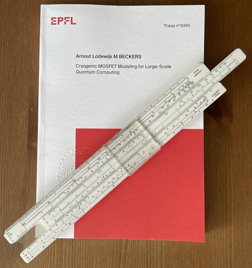
Arnout Lodewijk M BECKERS
Prof. E. Charbon, président du jury
Prof. C. Enz, directeur de thèse
Prof. B. Parvais, rapporteur
Prof. G. Ghibaudo, rapporteur
Dr J.-M. Sallese, rapporteur


#OpenPOWER Foundation | #Libre-SOC #180nm Power ISA ASIC Submitted to Imec for Fabrication https://t.co/S4K6p9gFcb #semi https://t.co/2yDUzjKJqN
— Wladek Grabinski (@wladek60) Jul 8, 2021

Special Issue on the 60th anniversary of the first laser Series I: Microcavity Photonics—from fundamentals to applications https://t.co/I9pRWzuxsQ #semi https://t.co/qW7HP2vfXd
— Wladek Grabinski (@wladek60) Jul 8, 2021
JFETLAB, has been updated to v1.2, supporting DC/CV simulations of Si and 4H-SiC lDG JFET; the mobility and intrinsic concentration doping/temperature and temperature dependence are incorporate, respectively. Gm/Id simulations are also included. https://t.co/C7RK06oWhD #semi https://t.co/hiW6NswqPP
— Wladek Grabinski (@wladek60) Jul 8, 2021


会议场所:西安电子科技大学北校区阶梯教学楼112报告厅,西安市雁塔区太白南路2号西安电子科技大学(北校区)No.2, South Taibai Road, Xian Dianzi University, Xi'an, 710071
Workshop Secretary: Meng Zhang Mobile:13619295980any related enquiries can be sent to registration@mos-ak.org


