Showing posts with label FDSOI. Show all posts

Mar 19, 2024

[Habilitation] Assessment of novel devices in CMOS technology

Assessment of novel devices in CMOS technology
by electrical characterization and physics-based model
Habilitation Presented To Obtain The Authorization 
To Direct Research From Sorbonne University
Lionel Trojman, PhD
Sorbonne Université, 2020
Organization of the thesis
Chapter 1: This chapter extends research work after the author’s PhD study. It focuses on HfO2-based dielectric MOSFETs with sub-1nm EOT. The study explores the impact of transport factors like saturation velocity on planar MOSFETs and the mobility of FDSOI-UTBB MOSFETs. Notably, the back-biased effect is considered, and an inversion charge model is developed for different front and back biases.
Chapter 2: Emphasis the application of the statistical defect-centric model to assess the impact of channel hot carriers on the reliability of low-dimensional MOSFETs.
Chapter 3: This chapter shifts focus to GaN-on-Si wafer devices for power electronic applications. These devices integrate MOS-like structures into III-V material-based devices, specifically MOS-HEMT and GET-SBD.
Chapter 4: Investigates RERAM devices. It stems from cooperative research with UNICAL and a PhD program in collaboration with Aix-Marseille University

FIG: Description of the gate structure (half device) of the studied device including the parasitic capacitance inner fringing (CIF), outer fringe (COF) and Junction overlap capacitance (COV)


Jun 13, 2023

[paper] FDSOI Threshold Voltage Model

Hung-Chi Han1, (Student, IEEE), Zhixing Zhao2, Steffen Lehmann2,
Edoardo Charbon1, (Fellow, IEEE), and Christian Enz1 (Life Fellow, IEEE)
Novel Approach to FDSOI Threshold Voltage Model Validated at Cryogenic Temperatures
in IEEE Access, DOI: 10.1109/ACCESS.2023.3283298

1 Ecole Polytechnique Fédérale de Lausanne (EPFL), 2000 Neuchâtel, Switzerland
2 GlobalFoundries, 01109 Dresden, Germany

Abstract: The paper presents a novel approach to to the modeling of the back-gate dependence of the threshold voltage of Fully Depleted Silicon-On-Insulator (FDSOI) MOSFETs down to cryogenic temperatures by using slope factors with a gate coupling effect. The FDSOI technology is well-known for its capability to modulate the threshold voltage efficiently by the back-gate voltage. The proposed model analytically demonstrates the threshold voltage as a function of the back-gate voltage without the pre-defined threshold condition, and it requires only a calibration point, i.e., a threshold voltage with the corresponding back-gate voltage, front- and back-gate slope factors, and work functions of front and back gates. The model has been validated over a wide range of the back-gate voltages at room temperature and down to 3 K. It is suitable for optimizing low-power circuits at cryogenic temperatures for quantum computing applications

FIG: Room temperature back-gate coefficient η versus VT−VB for an n-type conventional well (RVT) FDSOI FET with 1 µm of gate length and width. The θ=0 happens at VT−VB = −0.63V due to −0.63V of the front-back gate work function difference 

Acknowledgment: The authors would like to thank Claudia Kretzschmar from GlobalFoundries Germany and GlobalFoundries University Partnership Program for providing 22 FDX® test structures and support. Hung-Chi Han would like to thank Davide Braga from Fermi National Accelerator Laboratory for his valuable support. This project has received funding from the European Union’s Horizon 2020 Research & Innovation Program under grant agreement No. 871764. SEQUENCE.


Jan 5, 2022

[paper] A Review of Sharp-Switching Band-Modulation Devices

Sorin Cristoloveanu1, Joris Lacord2, Sébastien Martinie2, Carlos Navarro3, Francisco Gamiz3, Jing Wan4, Hassan El Dirani1, Kyunghwa Lee1 and Alexander Zaslavsky5
A Review of Sharp-Switching Band-Modulation Devices
Micromachines 2021, 12, 1540.
DOI: 10.3390/mi12121540
   
1 IMEP-LAHC, Université Grenoble Alpes (F)
2 CEA, LETI, MINATEC Campus (F)
3 CITIC-UGR, University of Granada (SP)
4 Fudan University, Shanghai (CN)
5 Brown University, Providence (US)


Abstract: This paper reviews the recently-developed class of band-modulation devices, born from the recent progress in fully-depleted silicon-on-insulator (FD-SOI) and other ultrathin-body technologies, which have enabled the concept of gate-controlled electrostatic doping. In a lateral PIN diode, two additional gates can construct a reconfigurable PNPN structure with unrivalled sharp-switching capability. We describe the implementation, operation, and various applications of these band-modulation devices. Physical and compact models are presented to explain the output and transfer characteristics in both steady-state and transient modes. Not only can band-modulation devices be used for quasi-vertical current switching, but they also show promise for compact capacitorless memories, electrostatic discharge (ESD) protection, sensing, and reconfigurable circuits, while retaining full compatibility with modern silicon processing and standard room-temperature low-voltage operation.


Fig: Average subthreshold swing SS vs. normalized ION plot. 
Green points indicate CMOS-compatible materials.

Acknowledgements: The European authors are grateful for support from the EU project REMINDER (H2020-687931). Alexander Zaslavsky acknowledges the support of the U.S. National Science Foundation (award QII-TACS-1936221).


Nov 9, 2021

8th EuroSOI-ULIS 2022 at University of Udine (Italy)

Organized by:
University of Udine (Italy)

Conference chair:
Pierpaolo Palestri

Local organizing Committee:
Francesco Driussi
David Esseni
Daniel Lizzit

Conference Secretariat:
Centro Congressi Internazionali 

Steering Committee:
  • Francis BALESTRA
    (IMEP Minatec, France)
  • Maryline BAWEDIN
    (IMEP-LAHC, France)
  • Cor CLAEYS
    (KU-Leuven, Belgium)
  • Bogdan CRETU
    (ENSICAEN, France)
  • Sorin CRISTOLOVEANU
    (IMEP-LAHC, France)
  • Francisco GAMIZ
    (UnivGranada, Spain)
  • Elena GNANI
    (Univ. of Bologna, Italy)
  • Benjamin INIGUEZ 
    (URV, Spain)
  • Joris LACORD
    (CEA-Leti, France)
  • Enrico SANGIORGI
    (Univ.Bologna, Italy)
  • Luca SELMI
    (Univ. of Modena, Italy)
  • Viktor SVERDLOV
    (TU Wien, Austria)
  • Andrei VLADIMIRESCU
    (ISEP, France)
Sponsors:


8th Joint International EuroSOI Workshop and International Conference
on Ultimate Integration on Silicon (EuroSOI-ULIS) 2022
May 18-20, 2022 – Udine, Italy

https://eurosoiulis2022.com

The Conference aims at gathering together scientists and engineers working in academia, research centers and industry in the field of SOI technology and nanoscale devices in More-Moore and More-Than-Moore scenarios. High quality contributions in the following areas are solicited:
  • Advanced SOI materials and structures, innovative SOI-like devices.
  • Alternative transistor architectures (FDSOI, Nanowire, FinFET, MuGFET, vertical MOSFET, FeFET and TFET, MEMS/NEMS, Beyond-CMOS).
  • New channel materials for CMOS (strained Si/Ge, III-V, carbon nanotubes; graphene and other 2D materials).
  • Properties of ultra-thin semiconductor films and buried oxides, defects, interface quality; thin gate dielectrics: high-κ and ferroelectric materials for switches and memory.
  • New functionalities and innovative devices in the More than Moore domain: nanoelectronic sensors, biosensor devices, energy harvesting devices, RF devices, imagers, integrated photonics (on SOI), etc.
  • Transport phenomena, compact modeling, device simulation, front- and back-end process simulation.
  • CMOS scaling perspectives; device/circuit level performance evaluation; switches and memory scaling; three-dimensional integration of devices and circuits, heterogeneous integration.
  • Advanced test structures and characterization techniques, parameter extraction, reliability and variability assessment techniques for new materials and novel devices.
Original 2-page abstracts with illustrations will be reviewed by the Scientific Committee. The accepted contributions will be published as 4-page letters in a special issue of the Elsevier journal Solid-State Electronics. Extended versions of outstanding papers will be published in a further special issue of Solid-State Electronics. A best poster award will be attributed by ELSEVIER. 

The “Androula Nassiopoulou Best Paper Award"
will be attributed by the SINANO institute.

Important dates:
  • abstract submission deadline: March 1, 2022
  • notification of acceptance: March 15, 2022

Nov 20, 2020

[paper] Characterization of ultrathin FDSOI devices using subthreshold slope method

Teimuraz Mchedlidze1, and Elke Erben2
Characterization of ultrathin FDSOI devices using subthreshold slope method
Phys. Status Solidi A. Accepted Manuscript
DOI: 10.1002/pssa.202000625

1 TU Dresden, Germany
2 Globalfoundries, Dresden, Germany

Abstract: The subthreshold current-voltage (subthreshold slope) characteristic of fully depleted silicon-on-insulator high-k dielectric-metal gate field-effect transistor is applied for evaluation of the interface traps located at both, the front and back channels. The proposed characterization method allows an estimation of averaged trap densities separately for the front and the back interfaces of the channel. Performing subthreshold slope measurements at several temperatures allow the extraction of the energy distributions of the interface trap densities for both interfaces and obtaining essential characteristics of the stack.

Fig: Results of ID(VGF,k,T) measurements for EG sample. At each temperature 
(200, 300 and 400K) a group of curves contains data for eight k values
(k = 0 to 3 with step 0.5 and kOC; solid curve). 

Acknowledgements: The authors would like to acknowledge funding of the study in the frames of the IPCEI WIN- FDSOI project from Global Foundries. We want to thank Jörg Weber (TU Dresden), Luca Pirro (Global Foundries) and Rolf Öttking (AQ Computare, Chemnitz) for thoughtful discussions and suggestions.


Sep 29, 2020

[thesis] RF UTBB FDSOI MOSFET

Vanbrabant, Martin
RF characterization of the back-gate contact on Fully Depleted SOI MOSFETs
http:// hdl.handle.net/2078.1/thesis:26763
Ecole polytechnique de Louvain, Université catholique de Louvain, 2020. 
Academic year 2019–2020: Master in Electrical Engineering
Prom.: Prof. Jean-Pierre Raskin
Readers: Denis Flandre, Valeriya Kilchytska, Lucas Nyssens, Martin Rack

Abstract: Thanks to the thin buried-oxide, the UTBB FDSOI technology with a highly doped region under the BOX is one of the main candidates for future RF applications. One of the most interesting feature of this technology is the possibility to tune the threshold voltage, compensate variability issues and improve the overall device performance. In this work, the impact of the back-gate bias is mainly studied on the threshold voltage and RF FoMs of the front and back-gates.


Figure: Reconstructed (dashed) vs initial (full) Re{Yij} insaturationat VDS=0.8V, VGS=0.8V and VB=0V for a 4-port device.


Jun 30, 2020

[webinar] Differentiated FDSOI for mmWave Solutions

WEBEX by IEEE EDS Santa Clara Valley/San Francisco Chapter

Differentiated Fully Depleted SOI (FDSOI) Technology 
for Highly Efficient and Integrated mmWave Wireless Connectivity Solution
Speaker: Dr. Anirban Bandyopadhyay,  Director, Strategic Marketing and Business Analytics, GLOBALFOUNDRIES, Inc., Santa Clara, CA
Friday, July 24, 2020 at 12PM – 1PM PDT

Abstract: The emergence of enhanced mobile broadband (eMBB) connectivity based on mmWave 5G and the emerging prospect of broadband internet to using non-terrestrial mmwave backhaul using low earth orbit (LEO) satellite generated huge interest in the entire telecommunication ecosystem. While mmwave allows huge bandwidth of channels to enable enhanced broadband, it also poses a lot of technical challenges in terms of coverage, generating enough transmitted power efficiently particularly in the uplink, system cost & scaling and long term reliability of the hardware system particularly for infrastructure including Satellite born systems. Current talk will focus on how Silicon technologies based on differentiated fully depleted SOI (FDSOI) can address the above challenges by enabling a highly efficient and integrated radio without compromising on the mmWave performance and reliability. Talk will highlight the technology Figures of Merits (FOMs) for a mmwave phased array system and how a differentiated FDSOI technology platform compares with other silicon technologies in terms of devices and circuits.

Speaker Bio: Dr. Anirban Bandyopadhyay is the Director, Strategic Marketing and Business Analytics within the Mobility & Wireless Infrastructure Business Unit of GLOBALFOUNDRIES, USA. His work is currently focused on hardware architecture & technology evaluations for emerging RF and mmWave applications. Prior to joining GLOBALFOUNDRIES, he was with IBM Microelectronics, New York and with Intel, California where he worked on different areas like RF Design Enablement, Silicon Photonics, signal integrity in RF & Mixed signal SOC’s. Dr. Bandyopadhyay did his PhD in Electrical Engineering from Tata Institute of Fundamental Research, India and Post-Doctoral research at Nortel, Canada and at Oregon State University, USA. He represents Global Foundries in different industry consortia on RF/mmWave applications and is a Distinguished Lecturer of IEEE Electron Devices Society.

More information at the IEEE EDS Santa Clara Valley-San Francisco Chapter Home Page

Subscribe or Invite your friends to sign up for our mailing list and get to hear about exciting electron-device relevant talks. We promise no spam and try to minimize email. You can unsubscribe easily.

Jun 15, 2020

[paper] Future of Ultra-Low Power SOTB CMOS

Nobuyuki Sugii1, Shiro Kamohara2, Makoto Ikeda3
The Future of Ultra-Low Power SOTB CMOS Technology and Applications
NANO-CHIPS 2030. The Frontiers Collection. Springer, Cham
DOI: 10.1007/978-3-030-18338-7_6
1.Hitachi, Ltd.Tokyo, Japan
2.Renesas Electronics Corp.Tokyo, Japan
3.The University of Tokyo, Japan

Abstract: Ultra-low power technology has drawn much attention recently as the number of connecting (Internet-of-Things) devices rapidly increases. The silicon-on-thin-buried oxide (SOTB) technology is a CMOS device technology that uses fully depleted silicon-on-insulator (FDSOI) transistors with a thin buried oxide layer enabling enhanced back-bias controllability and that can be monolithically integrated with the conventional bulk CMOS circuits. It can significantly reduce both the operation and the standby powers by taking advantage of low-voltage operation and back-biasing, respectively. In this chapter, advantages of the SOTB technology in terms of ultra-low power, circuits design and chip implementation examples including ultra-low power micro-controllers operating with harvested power, reconfigurable logic circuits, analog circuits, are reviewed, and a future perspective is shown.
Fig.: Schematic cross section of SOTB transistors. Hybrid bulk transistors are shown. SOTB  transistors are used in low-voltage (< ~1.5 V) logic and analog circuits including SRAMs. Bulk  transistors are used in peripheral, ESD-protection, high-voltage analog and power circuits, on-chip,  flash memory, and reuse of legacy circuits

Acknowledgements: The part of the work, especially on developing the SOTB technology by the Low-power Electronics Association and Project (LEAP), is supported by the Ministry of Economy, Trade and Industry (METI) and the New Energy and Industrial Technology Development Organization (NEDO). Part of the chip fabrication by the universities is done under a support of VLSI Design and Education Center (VDEC) in collaboration with Renesas Electronics Corporation, Cadence Corporation, Synopsys Corporation and Mentor Graphics Corporation.

May 15, 2020

[paper] Electrical characterization of advanced MOSFETs

Valeriya Kilchytska, Sergej Makovejev, Babak Kazemi Esfeh, Lucas Nyssens, Arka Halder,
Jean-Pierre Raskin and Denis Flandre
Electrical characterization of advanced MOSFETs towards analog and RF applications
IEEE LAEDC, San Jose, Costa Rica, 2020, 
doi: 10.1109/LAEDC49063.2020.9073536

Abstract - This invited paper reviews main approaches in the electrical characterization of advanced MOSFETs towards their target analog and RF applications. Advantages and necessity of those techniques will be demonstrated on different study cases of various advanced MOSFETs, such as FDSOI, FinFET, NW in a wide temperature range, based on our original research over the last years. 

URL: https://ieeexplore.ieee.org/stamp/stamp.jsp?tp=&arnumber=9073536&isnumber=9072949

Acknowledgements - This work was partially funded by Eniac “Places2Be”, Ecsel “Waytogofast”, FNRS - FRFC “Towards Highly-efficient 10 nm MOSFETs”, FP7 “Nanosil” and “Nanofunction” projects. The authors thank our colleagues from CEA-Leti, ST and Imec, and particularly, F. Andrieu, O. Faynot, T. Poiroux, S. Barraud, M. Haond, N. Planes, N. Collaert, C. Claeys, M. Jurczak, B. Parvais, R. Rooyackers, for providing UTBB FD SOI, NW and FinFET devices and valuable discussions.

Jul 23, 2019

[paper] A Surface-Potential-Based Analytical I-V Model of Full-Depletion Single-Gate SOI MOSFETs

1
Department of Electrical and Electronic Teaching, 
College of Information Science and Engineering, 
Huaqiao University, Xiamen 361021, China

2
Department of Electronic Engineering, Jinan University, Guangzhou 510632, China
*
Correspondence: yufei_jnu@126.com; Tel.: +86-0592-6162-385
These two authors contributed equally to this work.

Received: 10 May 2019 / Accepted: 12 June 2019 / Published: 14 July 2019
Electronics 20198(7), 785; https://doi.org/10.3390/electronics8070785

Abstract

: 
A surface-potential-based analytical I-V model of single-gate (SG) silicon-on-insulator (SOI) MOSFETs in full-depletion (FD) mode is proposed and compared with numerical data and Khandelwal’s experimental results. An explicit calculation scheme of surface potential, processing high computation accuracy and efficiency, is demonstrated according to the derivation of the coupling relation between surface potential and back-channel potential. The maximum absolute error decreases into 10−7 V scale, and computation efficiency is improved substantially compared with numerical iteration. Depending on the surface potential, the drain current is derived in closed-form and validated by Khandelwal’s experimental data. High computation accuracy and efficiency suggest that this analytical I-V model displays great promise for SOI device optimizations and circuit simulations.

Keywords:
 silicon-on-insulator MOSFETs; surface potential; back-channel potential; full-depletion; analytical I-V model
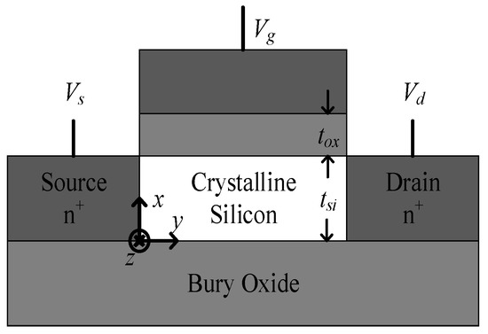
Figure 1. x-y cross section of silicon-on-insulator (SOI) MOSFETs.

Mar 16, 2015

[MOS-AK/DATE 2015 Workshop] CEA-Leti's predictive model takes FDSOI further

 CEA-Leti's predictive model takes FDSOI further 

During DATE 2015’s MOS-AK Workshop, CEA-Leti presented the newest version of its advanced compact model for ultra-thin body and buried oxide fully depleted SOI (UTBB-FDSOI) technology.

Fully Depleted Silicon On Insulator (FDSOI) is a planar process technology that relies on two primary innovations. First, an ultra-thin layer of insulator, called the buried oxide, is positioned on top of the base silicon.

Then, a very thin silicon film implements the transistor channel. Thanks to its thinness, there is no need to dope the channel, thus making the transistor fully depleted. The combination of these two innovations is called “ultra-thin body and buried oxide Fully Depleted SOI” or UTBB-FDSOI.

Back in 2013, CEA-Leti had deployed a first compact model, but working in close cooperation with STMicroelectronics, the research lab understood that more subtle back gate channelling effects had to be addressed to fully exploit the benefits of UTBB-FDSOI and to explore the transistors’ behaviour in more details.

New analytical equations were written from scratch for the Leti-UTSOI2.1 compact model, improving on the predictability and accuracy capabilities of the previous version, Leti-UTSOI2.

To date, other models from the University of Hiroshima, and from the University of Berkeley fail to account for inversion effects at the back interface, when a strong forward back bias (FBB) is applied, told us Thierry Poiroux, Leti research engineer and model co-developer.

More specifically, the French lab used a unique analytical resolution scheme for the calculation of surface potentials at both interfaces of the transistor body, offering a refined description of narrow-channel effects, with an improved accuracy of moderate inversion regime and gate tunnelling current modelling.

Because the model is analytical, it is much faster than any numerical simulation. It is now available in all major SPICE and Fast SPICE simulators through licences with EDA vendors and will allow fabless companies and IC designers to virtually explore different UTBB-FDSOI parameters within a given foundry process node. The new model can also be used by foundries and fabless companies to perform a predictive analysis of future nodes to come, in order to orient their ongoing process optimization.

for more information visit CEA-Leti at www.leti.fr