Aug 31, 2020

[JICS] SBMicro2020 Special Section Issue

Journal of Integrated Circuits and Systems
SBMicro2020 Special Section Issue
Vol 15 No 2 (2020)

The Journal of Integrated Circuits and Systems is an effort of both Brazilian Microelectronics Society - SBMicro and Brazilian Computer Society - SBC to create a new scientific journal covering intended to present state-of-art papers on Integrated Circuits and Systems, covering the fields of Process and Materials, Device and Characterization, Design, Test and CAD, among other relevant topics. The JICS is indexed in Scopus and Scimagojr.

SBMicro2020 Special Section Guest Editors:
Durga Misra, New Jersey Institute of Technology – NJIT, United States
Michelly de Souza, Centro Universitário FEI, Brazil

Online ISSN: 1872-0234 (from 2017 on)
Printed ISSN: 1807-1953 (prior to 2017)
Published: 2020-08-23


[paper] Bulk CMOS Technology at Sub-Kelvin Temperature

Characterization and Modeling of 0.18µm Bulk CMOS Technology 
at Sub-Kelvin Temperature 
Teng-Teng Lu1,2, Zhen Li1,2, Chao Luo1,2, Jun Xu2, Weicheng Kong3
and Guoping Guo1 (Member, IEEE) 
IEEE J-EDS, vol. 8, pp. 897-904, 2020
DOI: 10.1109/JEDS.2020.3015265.

1Key Laboratory of Quantum Information, University of Science and Technology of China, Hefei 230026, China 
2Department of Physics, University of Science and Technology of China, Hefei 230026, China 
3Department of Quantum Hardware, Origin Quantum Computing Company Limited, Hefei 230026, China

Abstract: Previous cryogenic electronics studies are mostly at 77K and 4.2K. Cryogenic characterization of a 0.18μm standard bulk CMOS technology (operating voltages: 1.8V and 5V) is presented in this paper. Several NMOS and PMOS devices with different width to length ratios (W/L) were extensively tested and characterized under various bias conditions at sub-kelvin temperature. In addition to devices dc characteristics, the kink effect and current overshoot phenomenon are observed and discussed at sub-kelvin temperature. Especially, the current overshoot phenomenon in PMOS devices at sub-kelvin temperature is shown for the first time. The transfer characteristics of MOSFET devices (1.8V W/L = 10μm/10μm) at sub-kelvin temperature are modeled using the simplified EKV model. This work facilitates the CMOS circuits design and the integration of CMOS circuits with silicon-based quantum chips at extremely low temperatures.
FIG: IDS-VGS curves of large thin TOX NMOS (a,b,e,f) and PMOS (c,d,g,h) devices at sub-kelvin temperature measured (symbols) and simulated (solid lines). 

Aknowlegement: This work was supported in part by the National Key Research and Development Program of China under Grant 2016YFA0301700, in part by the National Natural Science Foundation of China under Grant 11625419, in part by the Anhui initiative in Quantum information Technologies under Grant AHY080000, and in part by the USTC Center for Micro and Nanoscale Research and Fabrication.

[paper] Monolithic Pixel Detector in SOI Technology

High spatial resolution monolithic pixel detector in SOI technology 
R. Bugiela1, S. Bugiela2, D. Dannheimb, A. Fiergolskib, D. Hyndsb,3, M. Idzika, P. Kapustac, M. Munkerb, A. Nurnbergb4, S. Spannagelb,5, K. Swienteka, W. Kucewicza
aAGH-UST, Poland, bCERN, Switzerland, cIFJ PAN, Poland
CLICdp-Pub-2020-004
06 August 2020

1Present: CNRS/IPHC, France.
2Present: CNRS/IPHC, France.
3Present: NIKHEF, Amsterdam, Netherlands.
4Present: KIT, Karlsruhe, Germany.
5Present: DESY, Hamburg, Germany.

Abstract: This paper presents test-beam results of monolithic pixel detector prototypes fabricated in 200nm Silicon-On-Insulator (SOI) CMOS technology studied in the context of high spatial resolution performance. The tested detectors were fabricated on a 500µm thick highresistivity Floating Zone type n (FZ-n) wafer and on a 300 µm Double SOI Czochralski type p (DSOI Cz-p) wafer. The pixel size is 30µm×30µm and two different front-end electronics architectures were tested, a source follower and a charge-sensitive preamplifier. The test-beam data analyses were focused mainly on determination of the spatial resolution and the hit detection efficiency. In this work different cluster formation and position reconstruction methods are studied. In particular, a generalization of the standard η-correction adapted for arbitrary cluster sizes, is introduced. The obtained results give in the best case a spatial resolution of about 1.5µm for the FZ-n wafer and about 3.0µm for the DSOI Cz-p wafer, both detectors showing detection efficiency above 99.5%.

Fig.: Simplified schematics of Silicon-On-Insulator structures. The Buried N(P)-Well (BN(P)W) is a layer dedicated to shielding the electronics from the sensors electric field.

Aknowlegement: This work was financed by the European Union Horizon 2020 Marie Sklodowska-Curie Research and Innovation Staff Exchange program under Grant Agreement no. 645479 (E-JADE) and also by the Polish Ministry of Science and Higher Education from funds for science in the years 2017 – 2018 allocated to an international co-financed project. The authors would like to thank also the operators of the CERN SPS beam line and North Area test facilities.

Opinion Can Israel lead the #opensource code revolution? The Israeli tech scene is based on partnerships, innovation and independent thinking which are all vital in open-source code https://t.co/GdyYArG2sa https://t.co/yG6MPmp7bG


from Twitter https://twitter.com/wladek60

August 31, 2020 at 10:31AM
via IFTTT

Aug 28, 2020

TSMC: All the Processes, All the Fabs

TSMC Technology Symposium: All the Processes, All the Fabs
by Paul McLellan at breakfast-bytes
27 Aug 2020

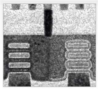
TSMC has new transistor structure (nanosheet) and new materials such as high mobility channel, 2D, carbon nanotube (CNT). TSMC has already demonstrated at 32Mb nanosheet SRAM fully-functional at 0.46V. It has also identified promising 2D materials such as MoS2 (molybdenum disulfide). At IEDM last year, they disclosed the first BEOL CNT power-gating device integrated with silicon-based CMOS.
Scaling continues with EUV advances with the current generation of scanners. They are also working with ASML (the only supplier of EUV equipment) on High-NA EUV [read more...]


Aug 27, 2020

Chip in the Fields: SBCCI and SBMicro Conferences

Chip in the Fields
C̶a̶m̶p̶i̶n̶a̶s̶,̶ ̶S̶P̶,̶ ̶B̶r̶a̶z̶i̶l̶ ̶ 
Virtual
August 24 to 28, 2020

Due to the COVID-19 pandemic the Chip in the Fields is changed to a virtual event. In 2021 we plan to have again the normal live Chip in the Fields events to be held in Hotel Premium, Campinas, SP, Brazil

The conferences SBCCI and SBMicro started in the early 80’s and since the year 2000 they joined forces, organizing them at the same venue and under a unified fantasy name “Chip in Somewhere”. The somewhere could be the name of the city or a fantasy name related to the region. It started with the name of “Chip in the Jungle”, because it was held in Manaus, the heart of the Amazon forest. 

Along these 21 years of Chip in, gradually other conferences joined the common venue and organization. Nowadays, we are composed of five sister conferences: SBCCI, SBMicro, WCAS, INSCIT and Sforum, as described in the respective call for papers. Due to the COVID-19 pandemic the Chip in the Fields is changed to a virtual event. Detalhes of the program and access link will be made available in the near future. Please follow the conference website for future up-dates.

Keynote Speakers

Kenneth K. O

Texas Analog Center of Excellence and Dept. of ECE,
The University of Texas at Dallas, Richardson, TX

Rajiv V. JoshiT. J. Watson research center, IBM                                         


Sponsored by:

Co-sponsored by:

Organized by:

Supported by:

Silicon Sponsors:

Platinum Sponsors:

Silver Sponsors:


Events:

Aug 26, 2020

[paper] SiC MOSFET Corner and Statistical SPICE Model Generation

SiC MOSFET Corner and Statistical SPICE Model Generation
Canzhong He, James Victory* , Yunpeng Xiao**, Herbert De Vleeschouwer+
Elvis Zheng++, ZhiPing Hu++ 
 ISPSD, September 13-18, 2020, Vienna, Austria
DOI: 10.1109/ISPSD46842.2020.9170091

   Power Design Enablement, ON Semiconductor, Mountain Top, Pennsylvania/USA
 *Power Design Enablement, ON Semiconductor, Aschheim, Germany
**Power Design Enablement, ON Semiconductor, Shanghai, China 
 +Wide Bandgap Technology Development, ON Semiconductor, Oudenaarde, Belgium 
++Product & Test Development Center, ON Semiconductor, Suzhou, China

Abstract: This paper presents a novel approach to generate corner and statistical SPICE models for SiC MOSFETs. The technique is derived from the mature IC industry standard approach known as Backward Propagation of Variance. Physically based, scalable SiC MOSFET SPICE models are required to simulate the correlations between electrical specifications and process variations. The methodologies presented are applicable to other power discrete devices such as super-junction MOSFETs, IGBTs, and GaN HEMTs.

Fig.: SiC MOSFET (a) Cross Section, (b) Subcircuit SPICE Model


Aug 25, 2020

[paper] Native High-k Oxides for 2D Transistors

Yury Yu. Illarionov1,2, Theresia Knobloch1 and Tibor Grasser1
Native high-k oxides for 2D transistors
Nature Electronics vol. 3, pp 442–443 (2020)
Published online: 05 August 2020
DOI: 10.1038/s41928-020-0464-2

1Institute for Microelectronics, TU Wien, Vienna, Austria
2Ioffe Physical-Technical Institute, St Petersburg, Russia

Abstract: The two-dimensional semiconductor Bi2O2Se can be oxidized to create an atomically thin layer of Bi2SeO5 that can be used as the insulator in scaled field-effect transistors.

Fig.: Development of FETs with Bi2O2Se channels and native Bi2SeO5 insulators. a.) Step-by-step oxidation of multilayer Bi2O2Se towards Bi2SeO5 and the crystal structure of the two materials. b.) Cross-sectional scanning transmission electron microscopy image confirming the atomically sharp interface. c.) Schematic of the top-gated devices fabricated with a native gate oxide. d.) Gate transfer characteristics of the devices with a 4.6-nm-thick Bi2SeO5 layer (EOT below 1 nm)

Analog IC Designer's Handbook

by Jean-Francois Debroux
 
Abstract: Analog IC design is one of the particular design activities where designers get feedback on their choices only months after they finish their design and where the cost of even the smallest design change is huge.
This has historically brought the need for new tools such as SPICE, the ancestor of almost all the electric simulators, so as to give feedback on the design choices before actually getting the prototypes. This should also have deeply impacted the design methods, and it has, but the availability of simulators has finally allowed the old “try and fix” method not only to survive but also to stay very popular.
If tools such as electric simulators have gained popularity in most electronic design fields, even out of the IC design world, methods such as the TOP-DOWN approach are not as popular as they should be, especially in the analog design community, even in the analog IC design microcosm. This is probably because this method is felt as difficult to use practically even though most designers agree that it is the right approach.
The goal of this book is to show that the TOP-DOWN approach for analog design is not only valid but that it is one of the most powerful available methods to create good analog design without sacrificing the time to market. This method creates faster and better designs but requires a good understanding of the method itself, of course, but also of the underlying techniques and of the basic design elements.
After a general introduction of the TOP-DOWN method goals and principles in the first part, the second part presents and details analog IC design elements from components to basic building blocks with a strong emphasis on practical aspects. Various additional design techniques are then detailed in the third part. The reader is then ready for the main course, a series of design examples based on the TOP-DOWN method that are grouped in the fourth part. These examples are processed the way they are in real life, from specification to implementation, from general considerations down to implementation details. Analysis of existing circuits is useful for learning but real life design is synthesis, not analysis.
Finally, the fifth part introduces or reminds useful basic concepts and presents the notation in use through the book.
The methods and techniques described in this book have been used by the author through 25 years of analog and mixed signal ICs design experience in various application fields including RF and sensor signal conditioning for various markets such as industrial, automotive and aerospace. The author feels that the method he presents in this book can help many analog electronic designers in their day to day work and hopes it will bring both a deeper understanding of design and a broader view over design activities. [read more...]

Experience: See  Jean-Francois Debroux profile on LinkedIn

Aug 24, 2020

Fwd: Announcement of Online Lecture Workshop On Frontiers in Science & Engineering - Opportunities for Graduates (Sept 14-19, 2020) jointly organized by Science Foundation and MHRD-IIC-DDUC Chapter, Deen Dayal Upadhyaya College, University of Delhi, New Delhi (Under the aegis of DBT Star College Program)

On behalf of Science Foundation and MHRD-IIC-DDUC Chapter, Deen Dayal Upadhyaya College, University of Delhi, New Delhi (Under the aegis of DBT Star College Program), I would like to invite you to kindly register for the Online Lecture Workshop On Frontiers in Science & Engineering - Opportunities for Graduates scheduled for September 14-19, 2020.

The workshop is likely to be supported by the Science Academies and will be organized using CISCO WEBEX/Microsoft Teams.

All Interested Science and Engineering Students and Faculty Members are requested to kindly register on 
or before August 25, 2020 via link appended below

There is NO REGISTRATION FEES. I request you to kindly motivate your students and colleagues to register for the same.


Organizing Committee
  • Professor Anurag Sharma, FNA, FNASc, FASc, FNAE, JC Bose National Fellow (SERB), Department of Physics, IIT Delhi (Convener-Workshop)
  • Professor Ajoy Ghatak, NASI Meghnad Saha Distinguished Professor, Chairperson-NASI Delhi Chapter.
  • Dr. Manoj Saxena, Coordinator-Workshop, Deen Dayal Upadhyaya College, University of Delhi, New Delhi (msaxena@ddu.du.ac.in)
  • Committee Members of Science Foundation, MHRD-IIC-DDUC Chapter and DBT Star College Program of  Deen Dayal Upadhyaya College, University of Delhi.
with regards

Dr. Manoj Saxena | डॉ मनोज  सक्सेना 
Associate Professor सह - आचार्य
Department of Electronics | इलेक्ट्रॉनिक्स विभाग
Deen Dayal Upadhyaya College | दीन दयाल उपाध्याय कॉलेज
University of Delhi | दिल्ली विश्वविद्यालय
Dwarka Sector-3, New Delhi-110078 | द्वारका क्षेत्र -, नई दिल्ली -११००७८
India | भारत

ResearcherID-Thomson Reuters : http://www.researcherid.com/rid/K-3863-2015 

Please do not print this email unless it is absolutely necessary. Spread environmental awareness. 

Fwd: IEEE-EDS Santa Clara Valley/San Francisco Chapter August Seminar (Webex only)

Please note that this seminar is now WEBEX participation only! 

Memory Errors in Production Systems – Insights from the Field
Speaker: Dr. Sudhanva Gurumurthi, Principal Member of Technical Staff, AMD
Friday, August 28, 2020 at 12PM – 1PM PDT

Abstract: Memory reliability is important for the correct operation of computing systems. While technology scaling has paved the way for improvements in the capacity and energy-efficiency of memory, the reliability aspects of such scaling must be well characterized and addressed in the design of computer hardware. AMD has collected and analyzed memory reliability data from several production systems running in data centers. This data spans several generations of DRAM technologies, as well as SRAM. This talk will first explain how bit-cell reliability can impact on the design and use of computing hardware and highlight the importance of studying memory faults from commercial hardware in the field. The talk will then present memory reliability data and insights from AMD's field studies and discuss their implications from the viewpoint architecting resilient systems.

Speaker Bio: Sudhanva Gurumurthi is a Principal Member of the Technical Staff at AMD, where he leads advanced development in Reliability, Availability, and Serviceability (RAS). He used to be an Associate Professor with tenure in the Computer Science Department at the University of Virginia. Sudhanva is a recipient of the NSF CAREER Award, a Google Focused Research Award, two Google Faculty Research Awards, and other NSF and industry awards. He is a Senior Member of the IEEE and the ACM. 

Subscribe or Invite your friends to sign up for our mailing list and get to hear about exciting electron-device relevant talks. We promise no spam and try to minimize email. You can unsubscribe easily.

To unsubscribe from the EDS-CHAP-SCV list, click the following link: https://listserv.ieee.org/cgi-bin/wa?SUBED1=EDS-CHAP-SCV&A=1

Aug 17, 2020

[paper] SPICE model of p‐Si TFET

Sola Woo Juhee Jeon Sangsig Kim 
A SPICE model of p‐channel silicon tunneling field‐effect transistors for logic applications
IJNM: 06 August 2020; DOI: 10.1002/jnm.2793

1Department of Electrical Engineering,Korea University, Seoul, South Korea

Abstract: In this study, we propose a SPICE model of p-channel silicon tunneling field-effect transistors (TFETs) for logic applications. To verify our model, electrical characteristics of fabricated p-TFETs are calibrated by utilizing TCAD and SPICE simulations. We simulate various logic gates, such as complementary TFET (c-TFET) inverters, c-TFET NAND gates, and c-TFET NOR gates using our TFET model. Our simulation shows that a c-TFET inverter can be operated at VDD as low as 0.3?V and that c-TFET logic gates based on our model can operate ~1000 times higher frequency than conventional TFET logic gates.
FIG: 2D structure of p-TFET for our simulation 
and its simulated/measured transfer characteristics at VDS=-1.0V

Acknowledgements: This research was partly supported by the MOTIE (Ministry of Trade, Industry & Energy) (10067791) and KSRC (Korea Semiconductor Research Consortium) support program for the development of the future semiconductor device, the Brain Korea 21 Plus Project in 2020, and Samsung electronics.

Aug 6, 2020

You don't need a computer science degree to work with #opensource software https://t.co/cpAlOk7V7U https://t.co/u3bNQ295sK


from Twitter https://twitter.com/wladek60

August 06, 2020 at 05:14PM
via IFTTT

[Call for Chapters] Sub-Micron Semiconductor Devices: Design and Applications

Call for Chapters
Title: Sub-Micron Semiconductor Devices: Design and Applications

Introduction: To follow Moore’s law, semiconductor devices are scaled-down without compromising the performance. Semiconductor devices are supposed to be reduced in dimensions and work at lower operating biases but the problem arises during the manufacturing of the devices. Thus, it is a dire necessity to opt for a solution that can help in continuing the path of performance improvement. Steady performance enhancement using optimization techniques can support the time required for advancements in fabrication technologies. This publication confines the novel semiconductor devices, issues with conventional devices, optimization techniques and solutions for the performance enhancement. Even with the presence of a vast amount of data regarding semiconductor devices, it is hard for a researcher to go through most of the recent advancements altogether and understand them in a clear way. The motive behind the book is to comprehensibly present the material related to the recent advancements in the field of semiconductor devices that can allow the reader to interpret the possible concepts behind the content. The study of novel semiconductor devices may help in unraveling the mystery behind the problems that are required to tackle during the fabrication of molecular devices.

Topics: [Not limited to the given topics but relevant topics will be considered as well]
  • Basic of Scaled-Down Devices
    • (Nano-FET, TFET, LED, Solar Cell, TFT, HEMT, Diodes, RTDs, Photodiode, Quantum-Dots, Spin-FET, etc.)
  • Comparative Study of Novel Semiconductor Devices
  • Inclusion of Quantum Effects in Nano-Devices
    • (Short Channel Effects, Fermi-Level-Pinning, Quantum Confinement, Discrete DOS, etc.)
  • Device Modelling and Physics
    • (Analytical, Compact, NEGF, Quantum, Verilog, Spice, etc.)
  • Novel Materials for Devices
    • (Graphene, Silicene, TMDCs, Organic, Perovskite, 2D Materials, TCO, Photo-dielectric, etc.)
  • Characterization and Fabrication
    • (Spectroscopic, Microscopic, MBE, CVD, Spin-Coating, Defects, etc.)
  • Optimization Techniques
    • (Negative Capacitance, Feedback, Gate-on-Source, Dopingless, 2DEG, Schottky Contact, etc.)
  • Testing of Semiconductor Devices
  • Applications
    • (Biosensor, Radiation Sensor, Light Sensor, Analog/Digital Circuit Applications, MEMS, etc.)
  • Issues and Solutions of Novel devices
  • Future Device Technology
Important Dates (Updated):
Chapter Proposal Submission: 10 September 2020
Notification of Acceptance: 15 September 2020
Full Chapter Submission: 25 October 2020
Review Result Returned: 30 October 2020
Final Acceptance: 10 November 2020
Publication of Book: January-February 2021

Submission:
Kindly submit the chapter proposal [Tittle, Abstract (500-1000 words), Possible Content, Author details] before the due date via E-mail at call.chapters.crc@gmail.com. Any kind of query regarding the chapter or abstract submission, formatting and corrections can be submitted to query.chapters.crc@gmail.com
Editors:
Ashish Raman1, Deep Shekhar2 and Naveen Kumar3
Electronics and Communication Engineering Department, Dr. B. R. Ambedkar National Institute of Technology Jalandhar, [Grand Trunk Road, Barnala - Amritsar Bypass Rd, Jalandhar, India 144011] 
Official E-mail IDs: 1 ramana@nitj.ac.in, 2 deeps.ec.18@nitj.ac.in, 3 naveenk.ec.16@nitj.ac.in


[chapter] Design of FET Biosensors

Khuraijam Nelson Singh1 and Pranab Kishore Dutta1
Chapter 8: Analytical Design of FET-Based Biosensors
in Advanced VLSI Design and Testability Issues; Eds: Suman Lata et all.
CRC Press, 19 Aug 2020; 360 pages

1NERIST, Arunachal Pradesh, India

Abstract: Research on biosensors has seized the interested researchers over the past few decades due to their various advantages and applications. They are used in the discovery of drugs, monitoring of diseases, agriculture, food quality control, industrial wastage monitoring, military, etc. The sensing analyte is the main element that differentiates a biosensor from the other physical/chemical sensors. In general, the biosensor is a device that is used to detect an analyte using a biosensitive receptor. Its main components are as follows:
  • Analytes: The substance that is intended to be detected, such as glucose in a glucose sensor, ammonia in ammonia sensor, and so on.
  • Bioreceptors: The bioreceptors are biosensitive elements used to detect target analytelbiomolecule. They are sensitive to the analytes of interest. Some examples of bioreceptors are antigen, DNA, enzyme, and so on.
  • Transducers: The elements that are used to convert energy from one form to another are called transducers. In a biosensor, the interaction of analytes and bioreceptors produces changes in the form of heat, gas, light, ions, or electrons. These changes are then converted into a quantif‌iable form by the transducer. Usually, the output of the transducer is in the form of electrical or optical signals, and the generated signal is proportional to the interaction between the analyte and the biosensor.
FIG: Schematic diagram of ion-sensitive f‌ield-effect transistor (ISFET)

Aug 5, 2020

[paper] GCC Method for Determining MOSFET VTH

Matthias Bucher1, Nikolaos Makris1, Loukas Chevas1
Generalized Constant Current Method for Determining MOSFET Threshold Voltage
arXiv:2008.00576v1 (2 Aug 202) 
has been submitted to the IEEE for possible publication

1 School of Electrical and Computer Engineering, Technical University of Crete

Abstract: A novel method for extracting threshold voltage (VTH) and substrate effect parameters of MOSFETs with constant current bias at all levels of inversion is presented. This generalized constant-current (GCC) method exploits the charge-based model of MOSFETs to extract threshold voltage and other substrate-effect related parameters. The method is applicable over a wide range of current throughout weak and moderate inversion and to some extent in strong inversion. This method is particularly useful when applied for MOSFETs presenting edge conduction effect (subthreshold hump) in CMOS processes using Shallow Trench Isolation (STI).
Fig:  Application of the GCC method in presence of edge conduction phenomenon in STI MOSFETs. A constant current is applied to determine pinchoff voltage for the center transistor in moderate inversion at IC=2. To characterize the edge transistor, imposing a current criterion IC=1E−4 corresponds to ICe≈0.02. Pinchoff voltage (VP) and slope factor n characteristics illustrate the determination of parameters for center and edge transistors.

Acknowledgment: This work was partly supported under Project INNOVATION-EL-Crete
(MIS 5002772).


#Top10 #Analogue Companies https://t.co/AOW7Q1A4Ou #semi https://t.co/Zzt1sVsobD


from Twitter https://twitter.com/wladek60

August 05, 2020 at 10:06AM
via IFTTT

[paper] Macromodels for MEMS Switches

Aurel-Sorin Lup1, Gabriela Ciuprina1, Daniel Ioan1 and Anton Duca1
and Alexandra Nicoloiu2 and Dan Vasilache2
Physics-aware macromodels for MEMS switches
COMPEL International Journal (2020)

1DEE Politehnica, Uni. Bucharest, (R)
2IMT-Bucharest, Bucharest (R)

Abstract: The purpose of this paper is to propose a physics-aware algorithm to obtain radio frequency (RF)- reduced models of micro-electromechanical systems (MEMS) switches and show how, together with multiphysics macromodels, they can be realized as circuits that include both lumped and distributed parameters. The macromodels are extracted with a robust procedure from the solution of Maxwell’s equations with electromagnetic circuit element (ECE) boundary conditions. The reduced model is extracted from the simulations of three electromagnetic field problems, in full-wave regime, that correspond to three configurations: signal lines alone, switch in the up and down positions. The technique is exemplified for shunt switches, but it can be extended for lateral switches. Moreover, the algorithm is able take frequency dependence into account both for the signal lines and for the switch model. For the later, the order of the model is increased until a specified accuracy is achieved. The use of ECE as boundary conditions for the RF simulation of MEMS switches has the advantage that the definition of ports is unambiguous and robust as the ports are clearly defined. The extraction approach has the advantage that the simplified model keeps the basic phenomena, i.e. the propagation of the signal along the lines. As the macromodel is realized with a netlist that uses transmission lines models, the lines’ extension is natural. The frequency dependence can be included in the model, if needed.

Fig: Modeling chain: from continuous models to reduced macromodels

Acknowledgement: The work has been funded by the Operational Programme Human Capital of the Ministry of European Funds through The Financial Agreement 51675/09.07.2019, SMIS code 125125.


Aug 4, 2020

William English, Computer Mouse Co-Creator, Has Passed died July 26 in San Rafael, California. He was 91 years old. https://t.co/q7PNnR694g #semi https://t.co/KOCm8at33a


from Twitter https://twitter.com/wladek60

August 04, 2020 at 03:37PM
via IFTTT

[paper] SiC MOSFET SPICE Model

Lefdal Hove, Haavard, Ole Christian Spro, Giuseppe Guidi
and Dimosthenis Peftitsis
Improved SiC MOSFET SPICE Model to Avoid Convergence Errors
Materials Science Forum 1004 (July 2020): 856–64
DOI: 10.4028/www.scientific.net/msf.1004.856

Abstract: This paper presents improvements to a SPICE model for a commercially available SiC MOSFET to avoid convergence errors while still providing reliable simulation results. Functionality in the internal part of the model that shapes the transconductance of the device according to its junction temperature and gate-source voltage dependency has been improved to provide a continuous characteristic rather than the initial discontinuous performance. Furthermore, the output characteristics from the initial and the proposed model have been compared to lab measurements of an actual device. The results show that the proposed and initial model provide equally reliable simulation results. However, the proposed model does not run into convergence problems.

References 
[1] X. She, A. Huang, O. Lucia, and B. Ozpineci, Review of Silicon Carbide Power Devices and Their Applications, IEEE Transactions on Industrial Electronics, vol. 64, no. 10, p.8193–8205, (2017).
[2] J. Rabkowski, D. Peftitsis, and H. P. Nee, Silicon carbide power transistors: A new era in power electronics is initiated, IEEE Industrial Electronics Magazine, vol. 6, no. 2, p.17–26, (2012).
[3] A. Stefanskyi, L. Starzak, A. Napieralski, and M. Lobur, Analysis of SPICE models for SiC MOSFET power devices,, 2017 14th CADSM 2017 - Proceedings, p.79–81, (2017).
[4] H. L. Hove, O. C. Spro, D. Peftitsis, G. Guidi, and K. Ljøkelsøy, Minimization of dead time effect on bridge converter output voltage quality by use of advanced gate drivers, 2019 10th ICPE 2019 ECCE Asia, (2019).
[5] N. Mohan, T. Undeland, and W. Robbins, Power Electronics; Converters, Applications, and Design, third ed., Wiley, (2003).
[6] C. Enz, F. Krummenacher, and E. Vittoz, An Analytical MOS Transistor Model Valid in All Regions of Operation and Dedicated to Low-Voltage and Low-Current Application, Analog Integrated Circuits and Signal Processing, vol. 8, p.83–114, (1995).
[7] M. Bucher, C. Lallement, C. Enz, F. Théodoloz, and F. Krummenacher, The EPFL-EKV MOSFET Model Equations for Simulation Technical Report V2.6,, EPFL, Lausanne, Switzerland, (1999).
[8] B. N. Pushpakaran, S. B. Bayne, G. Wang, and J. Mookken, Fast and accurate electro-thermal behavioral model of a commercial SiC 1200V, 80 mΩ power MOSFET,, Digest of Technical Papers IEEE IPPC, vol. 2015-Octob, p.1–5, (2015).

Aug 3, 2020

IEEE International Electron Devices Meeting to be Held Virtually https://t.co/LGJVdu1TyN https://t.co/vVgVsLrX4I #paper https://t.co/XN5oesBAQE


from Twitter https://twitter.com/wladek60

August 03, 2020 at 06:10PM
via IFTTT

#Samsung wants consortium, not #Nvidia, to buy #ARM https://t.co/oHWncoirCL #semi https://t.co/ugfrenqdAX


from Twitter https://twitter.com/wladek60

August 03, 2020 at 05:15PM
via IFTTT

#SMIC, #Beijing to build $7.6 billion #wafer fab https://t.co/ZqczycwQXx #semi https://t.co/VNhsMxR6zX


from Twitter https://twitter.com/wladek60

August 03, 2020 at 01:42PM
via IFTTT