Showing posts with label mos-ak. Show all posts

Aug 14, 2023

[11k online viewers] 7th Sino MOS-AK/Nanjing

Arbeitskreis Modellierung von Systemen und Parameterextraktion
Modeling of Systems and Parameter Extraction Working Group
7th Sino MOS-AK Workshop in Nanjing (CN)
August 11-13, 2023 (online/onsite)
Recent, consecutive, 7th Sino MOS-AK/Nanjing Workshop discussing the Compact/SPICE modeling and its Verilog-A Standardization reached 11k online viewers. The MOS-AK participants and online attendees have followed one day SiC-related device modeling training on August 11 featured presentations by experts currently working at Robert Bosch GmbH and then two days workshop with 24 R&D Compact/SPICE modeling presentations:


May 17, 2022

[mos-ak] [2nd Announcement and C4P] 4th International MOS-AK/LAEDC Workshop July 3 Puebla (MX)


2nd Announcement and C4P

Together with local online host, the LAEDC Organizers as well as all the Extended MOS-AK TPC Committee, would like to invite you to the 4th International MOS-AK/LAEDC Workshop which will be organized as the virtual/online event on July 3  between 8:30am -  12:30pm (UTC/GMT -5 hours) as a hybrid event in Puebla (MX) providing an opportunity to meet with modeling engineers and researchers from Europe and Latin America.

Upcoming MOS-AK/LAEDC Workshop aims to strengthen a network and discussion forum among experts in the field, enhance an open platform for information exchange related to compact/SPICE modeling and Verilog-A standardization, bring academic and industrial experts in the compact modeling field together, as well as obtain feedback from technology developers, circuit designers, and CAD/EDA tool developers and vendors, in particular using Free 130nm Skywater PDK.

Topics to be covered include the following among other related to the compact/SPICE modeling and its Verilog-A standardization:
  • Compact Modeling (CM) of the electron devices
  • Advances in semiconductor technologies and processing
  • Verilog-A language for CM standardization
  • New CM techniques and extraction software
  • Open Source (FOSS) TCAD/EDA modeling and simulation
  • CM of passive, active, sensors and actuators
  • Emerging Devices, Organic TFT, CMOS and SOI-based memory
  • Microwave, RF device modeling, high voltage device modeling
  • Nanoscale CMOS, BiCMOS, SiGe, GaN, InP devices and circuits
  • Technology R&D, DFY, DFT and reliability/aging IC designs
  • Foundry/Fabless Interface Strategies (eg: Skywater 130nm CMOS)
List of MOS-AK speakers (tentative in alphabetical order) :
  • Sergio Bampi, UFRGS (BR)
  • Juan Brito, IMPINJ (BR)
  • Antonio Cerdeira, CINVESTAV (MX)
  • Benjamin Iniguez, URV (SP)
  • Roberto Murphy, INAOE (MX)
  • Jean-Michel Sallese, EPFL (CH)
  • Gilson I Wirth, UFRGS (BR)
Online Abstract Submission is open (any related enquiries can be sent to abstracts@mos-ak.org)
Online Event Registration is open (any related enquiries can be sent to registration@mos-ak.org)

Important Dates: 
    • Call for Papers: Dec. 2021
    • 2nd Announcement: May 2022
    • Final Workshop Program: June 2022
    • MOS-AK: July 3 2022, Puebla (MX)
      • 8:30am - 12:30pm (UTC/GMT -5 hours) MOS-AK Workshop
    W.Grabinski for Extended MOS-AK Committee

    WG170522


    Apr 19, 2021

    [Photos] MOS-AK LADEC Mexico April 18, 2021

    Arbeitskreis Modellierung von Systemen und Parameterextraktion
    Modeling of Systems and Parameter Extraction Working Group
    MOS-AK LAEDC Workshop
    (virtual/online) April 18, 2021

    Together with local Host and LAEDC Organizers as well as all the Extended MOS-AK TPC Committee, we have organized the 3rd subsequent MOS-AK/LAEDC workshop which was the Virtual/Online event. There are a couple of the event photos:

    MOS-AK Session 1 (APR.18) begun: 8:00am Mexico time zone (GMT-5)

    T_1 FOSSEE eSIM: An open source CAD software for circuit simulation
    Kannan Moudgalya
    IIT Bombay (IN)

    T_2 Memristor modeling
    Arturo Sarmiento
    INAOE (MX)

    T_3 Modeling Issues for CMOS RF ICs
    Roberto Murphy, Jose Valdes and Reydezel Torres
    INAOE (MX)

    T_4 Improving Time-Dependent Gate Breakdown of GaN HEMTs with p-type Gate
    E. Sangiorgi, A. Tallarico, N. Posthuma, S. Decoutere, C. Fiegna
    Universita di Bologna

    MOS-AK Session 2 (APR.18) begun: 1:00pm Mexico time zone (GMT-5)

    T_5 Compact Models of SiC and GaN Power Devices
    Alan Mantooth, Arman Ur Rashid, Md Maksudul Hossain
    University of Arkansas (US)

    T_6 New analytical model for AOSTFTs
    Antonio Cerdeira
    CINVESTAV-IPN, Mexico City (MX)

    T_7 On the Parameter Extraction of Thin-Film Transistors in Weak-Conduction
    Adelmo Ortiz-Conde
    Solid State Electronics Laboratory, Simon Bolivar University, Caracas (VE)

    End of MOS-AK Workshop
    Group Photo


    Apr 7, 2021

    [paper] Compact Modeling as a Bridge between Technologies and ICs


    Compact Modeling as a Bridge 
    between Scaled Semiconductor Technologies and Advanced Designs of the Integrated Circuits
    AB Bhattacharyya and Wladek Grabinski
    IETE Journal of Research 58(3):179-180 (May 2012)
    DOI: 10.4103/0377-2063.97322

    Abstract: The quality of the integrated circuits analysis, required in present contemporary design flows, is directly linked to the accuracy of its basic components—the Compact Model/Simulation Program with Integrated Circuit Emphasis (SPICE) Model. The compact/SPICE modeling is an essential research activity bridging scaled semiconductor technologies and advanced designs of the integrated circuits. To enable complete access to the new advanced semiconductor technologies, the designers have to frequently update their Computer-Aided Design (CAD) tools with accurate definition of the semiconductor device models that can be implemented into the CAD circuit simulators. The models must preferably be physics-based to account for complex dependencies of the device properties and defined in standard, high-level language, i.e., Verilog-A, to simplify access and implementation into the CAD tools. For the state of the art advanced CMOS technologies (analog, HV, SOI), both modeling and characterization are challenging tasks that will be emphasized in this special issue of Compact Modeling. (REF) Compact Modeling as a Bridge between Scaled Semiconductor Technologies and Advanced Designs of the Integrated Circuits. 

    Available from: <http://www.mos-ak.org/india/>
    and https://www.researchgate.net/publication/278384752_Compact_Modeling_as_a_Bridge_between_Scaled_Semiconductor_Technologies_and_Advanced_Designs_of_the_Integrated_Circuits

    Mar 23, 2021

    [mos-ak] [2nd Announcement and C4P] 3rd MOS-AK LAEDC Workshop (virtual/online) April 18, 2021

    2nd Announcement and C4P

    Together with  local organization team, International MOS-AK Board of R&D Advisers as well as all the Extended MOS-AK TPC Committee, we have the pleasure to invite to 3rd consecutive MOS-AK Compact/SPICE Modeling Workshop which will be organized as the virtual/online event on April 18, 2021 preceding the LAEDC Conference.

    Planned virtual 3rd MOS-AK LAEDC Workshop aims to strengthen a network and discussion forum among experts in the field, enhance open platform for information exchange related to compact/SPICE modeling and Verilog-A standardization, bring academic and industrial experts in the compact modeling field together, as well as obtain feedback from technology developers, circuit designers, and CAD/EDA tool developers and vendors.

    Venue: Virtual/Online at LAEDC Conference

    Online Workshop Registration to be in April 2021, 
    any related enquiries can be sent to registration@mos-ak.org

    Topics to be covered include the following among other related to the compact/SPICE modeling and its Verilog-A standardization:
    • Compact Modeling (CM) of the electron devices
    • Advances in semiconductor technologies and processing
    • Verilog-A language for CM standardization
    • New CM techniques and extraction software
    • Open Source (FOSS) TCAD/EDA modeling and simulation
    • CM of passive, active, sensors and actuators
    • Emerging Devices, Organic TFT, CMOS and SOI-based memory cells
    • Microwave, RF device modeling, high voltage device modeling
    • Nanoscale CMOS, BiCMOS, SiGe, GaN, InP devices and circuits
    • Technology R&D, DFY, DFT and reliability/aging IC designs
    • Foundry/Fabless Interface Strategies
    Online Abstract Submission to be open, 
    any related enquiries can be sent to abstracts@mos-ak.org

    Important Dates: 
    • Call for Papers - Dec. 2020
    • 2nd Announcement - March 2020
    • Final Workshop Program - April 2020
    • MOS-AK Workshop April 18, 2021

    WG23032021

    --
    You received this message because you are subscribed to the Google Groups "mos-ak" group.
    To unsubscribe from this group and stop receiving emails from it, send an email to mos-ak+unsubscribe@googlegroups.com.
    To view this discussion on the web visit https://groups.google.com/d/msgid/mos-ak/CALp-Rj_qCy53wUsXOkXoAgCCS7-FCHgHfGkeEyYsuPJtXx2Qiw%40mail.gmail.com.

    Feb 26, 2021

    [DAY 2] 1st Asia/South Pacific MOS-AK Workshop

    Arbeitskreis Modellierung von Systemen und Parameterextraktion
    Modeling of Systems and Parameter Extraction Working Group
    1st Asia/South Pacific MOS-AK Workshop
    (virtual/online) FEB. 25-26, 2021

    Day2: FEB.26
    Session C Chair: Sadayuki Yoshitomi, Kioxia (J)

    [8] eSim: An open source CAD software for circuit simulation
    Kannan Moudgalya
    IIT Bombay (IN)

    [9] A modular approach to next generation Qucs
    Felix Salfelder and Mike Brinson
    QUCS Team; Centre for Communications Technology, London Metropolitan University (UK)

    [12] Machine learning-based approach to model and analyze GaN power devices
    Tian-Li Wu
    National Yang Ming Chiao Tung University, Taiwan (TW)

    [11] TCAD-inspired compact modeling approach
    Sung-Min Hong and Kwang-Woon Lee
    Gwangju GIST (KR)

    Session D Chair: Sheikh Aamir Ahsan, NIT Srinagar (IN)
    [10] An Innovative Technique for Ultrafast Carrier Dynamics and THz Conductivities of Semiconductor Nanomaterials
    Praveen Kr. Saxena and Fanish Kr. Gupta
    Tech Next Lab, Lucknow (IN)

    [13] Compact Modeling of 3D NAND Flash Memory for Diverse Unconventional Analog Applications
    Shubham Sahay
    IIT Kanpur (IN)

    [14] Steep Subthreshold Slope PN-Body Tied SOI-FET for Ultralow Power LSI, Sensor, and Neuromorphic Chip
    Takayuki Mori and Jiro Ida
    Kanazawa Institute of Technology, Nonoichi (J)

    [Pic] Group photo of selected MOS-AK participants attending 2nd Day of the workshop


    [DAY 1] 1st Asia/South Pacific MOS-AK Workshop

    Arbeitskreis Modellierung von Systemen und Parameterextraktion
    Modeling of Systems and Parameter Extraction Working Group
    1st Asia/South Pacific MOS-AK Workshop
    (virtual/online) FEB. 25-26, 2021

    DAY 1: FEB. 25, 2021
    Session A Chair: Usha Gogineni, ams AG, Hyderabad (IN)

    [1] New Insights in Low Frequency Noise Characteristics in PE-BJTs
    Peijian Zhang and Ma Long
    Science and Technology on Analog Integrated Circuit Laboratory; WHU (CN), Keysight Technologies (US)

    [2] Direct white noise characterization of short-channel MOSFETs
    K. Ohmori and S. Amakawa
    DeviceLab, Tsukuba (J)

    [3] SPICE Modeling of 2D-material based FETs with Schottky-barrier contacts
    Sheikh Aamir Ahsan
    Nanoelectronics Research and Development Group, NIT Srinagar, Jammu and Kashmir (IN)


    [4] Physics-based model of SiC MOSFETs including high voltage and current regions
    Sourabh Khandelwal, Cristino Salcines, and Ingmar Kallfass
    Macquarie University Sydney (AU), University of Stuttgart (D)

    Session B Chair: Daniel Tomaszewski, IMiF, Warszaw (PL)
    [5] Compact Modeling for Gate-All-Around FET Technology
    Avirup Dasgupta
    IIT Roorkee (IN)


    [6] BSIM-HV: Advanced High Voltage MOSFET Compact Model
    Harshit Agarwal
    IIT Jodhpur (IN)

    [7] ASCENT+ Transnational Access for the nanoelectronics
    Georgios Fagas
    Tyndall (IE)

    [Pic] Group photo of selected MOS-AK participants attending 1st Day of the workshop

    Jan 22, 2021

    Joint Spring MOS-AK, SB-MOS and IEEE EDS MQ

    Joint Spring MOS-AK Workshop and Symposium on Schottky Barrier MOS (SB-MOS) Devices
    with IEEE EDS Mini-Colloquium on “Non-Conventional Devices and Technologies”
    September 29 to October 1, 2020
    THM Giessen (Germany)
    —by Mike Schwarz— The Joint Spring MOS-AK Workshop and Symposium on Schottky Barrier MOS (SB-MOS) devices with IEEE EDS Mini-Colloquium on “Non-conventional Devices and Technologies” was held from September 29 to October 1, 2020. While it was initially planned for spring at THM—University of Applied Sciences in Giessen (Germany), it was shifted to the early autumn due to the COVID-19 pandemic. However, finally the local organizers of NanoP Competence Center for Nanotechnology and Photonics of THM decided to move it to Zoom and perform it virtually. It was sponsored by THM, the EDS Germany Chapter, the IEEE Young Professionals Germany Affinity Group, and the AdMOS company. The event was attended by 69 IEEE members and 115 non IEEE members (guests) from 25 countries during the three days [read more...]

    Dec 12, 2020

    [2nd Day Photos] 13th International MOS-AK Workshop

    13th International MOS-AK Workshop was organized jointly with THM Giessen who has provided ZOOM meeting platform for the online event. 50+ registered participants have attended 2nd day with two further MOS-AK sessions and followed 7 technical talks

    MOS-AK session III - 11:00 - 14:00 (PST) on Dec.11, 2020
    Chair: Anurag Mangla; Semtech Neuchatel (CH)

    [8] Statistical Analysis of MOSFET extracted parameters for n-MOS mismatch modeling.
    Juan Pablo Martinez Brito
    CEITEC SA/UFRGS (BR)

    [9] Rapid multiscale simulation of nanoscale MOSFETs: Is an interplay between compact models and NEGF possible?
    Alexander Kloes
    NanoP, THM University of Applied Sciences (D)


    [10] The Effect of Non Rectangular MOS Channels in Modelling High Voltage Lateral MOS
    Marco Sambi, Lorenzo Labate, Simona Cozzi, Nicola Holzer
    STMicroelectronics (I)

    MOS-AK session IV
    Chair: Daniel Tomaszewski, Lukasiewicz - IMiF, Warsaw (PL)

    [11] Nonlinear Embedding Model for the Accelerated Design of PAs with the ASM-HEMT model
    Patrick Roblin*, Miles Lindquist*, Nicholas Miller+ and Marek Mierzwinski^
    *The Ohio State University, AFRL+, Keysight Corp.^ (USA)

    [12] New analytical model for AOSTFTs
    Antonio Cerdeira, Yoanlys Hernandez-Barrios, Magali Estrada, Benjamin Iniguez
    CINVESTAV (MX) and URV (SP)

    [13] Unifying the Modeling of Charge Trapping in RTN, 1/f Noise and BTI
    Gilson Wirth
    UFRGS (BR)

    [14] SPICE Modeling for Display Technologies
    Bogdan Tudor
    Silvaco (USA)

    MOS-AK attendees group photo of 2nd MOS-AK workshop day:

    MOS-AK attendees group photo (1)

    MOS-AK attendees group photo (2)


    Jun 9, 2020

    Virtual Education Events at ESSDERC/ESSCIRC 2020


    Given this uncertain situation, the organizing committee of ESSDERC/ESSCIRC 2020 in Grenoble and its Steering Committee, have decided to propose a new format for coming conference, which will include a NEW and Virtual Education Event series being developed for September 14th 2020 consisting of 13 educational sessions (workshops and tutorial) comprising invited presentations by leading academic and industrial experts and technologists. All related technical program details are also available online: https://www.esscirc-essderc2020.org/educationals

    1. TUTORIAL | Quantum Computing: Myth or Reality?
    Chairs: M. Vinet (CEA) and Farhana Sheikh (Intel)
    Full content duration ~6h
    2. WORKSHOP | Emerging Solutions for Imaging Devices, Circuits and Systems
    Chairs: Matteo Perenzoni (FBK) and Albert Theuwissen (Harvest Imaging)
    Full content duration ~6h
    3. WORKSHOP | Non-Volatile Memories: Opportunities and Challenges from Devices to Systems
    Chairs: Gabriel Molas (CEA) and Mahmut Sinangil (TSMC)
    Full content duration ~6h
    4. WORKSHOP | New 5G integration solutions, and related technologies (from materials to system)
    Chairs: Nadine Collaert (imec) and Stefan G. Andersson (Ericsson)
    Full content duration ~6h
    5. WORKSHOP | Advances in device technologies for automotive industry (power devices, SiC, GaN)
    Chairs: Ionut Radu (Soitec) and Stefaan Decoutere (IMEC)
    Full content duration ~6h
    6. WORKSHOP | Embedded monitoring and compensation design for energy or safety constrained applications
    Chairs: Sylvain Clerc (ST) and Keith Bowman (Qualcomm)
    Full content duration ~4h
    7. WORKSHOP | Edge AI and In-Memory-Computing for energy efficient AIoT solutions​
    Chairs:  Andreas Burg (EPFL) and Marian Verhelst (KUL)
    Full content duration ~6h
    8. WORKSHOP | Ab-initio simulations supporting new materials & process developments
    Chairs: Denis Rideau (ST) and Philippe Blaise (Silvaco)
    Full content duration ~3h
    9. WORKSHOP | RISC-V cooking session
    Chairs: Bora Nikolic (BWRC)
    Full content duration ~3h
    10. DISSEMINATION WORKSHOP |  Toward sustainable IOT from rare materials to big data
    Chairs:  Thierry Baron (CEA, LTM/UGA) and Audrey Dieudonné (UGA)
    Full content duration ~3h
    11. DISSEMINATION WORKSHOP | High Density 3D CMOS Mixed-Signal Opportunities
    Chair: Philipp Häfliger (UiO)
    Full content duration ~3h
    12. MOS-AK WORKSHOP | Compact/SPICE Modeling and its Verilog-A Standardization
    Chair: Wladek Grabinski (MOS-AK) and Daniel Tomaszewski (ITE Warsaw)
    Full content duration ~6h
    13. IPCEI on Microelectronics: Innovative Technologies for Shaping the Future
    Chairs: Dominique Thomas (ST), Klaus Pressel (Infineon), Rainer Pforr (Zeiss)
    Full content duration ~6h

    Nov 19, 2019

    MOS-AK India #45395 is now published in IEEE Xplore

    2019 IEEE Conference on Modeling of Systems Circuits and Devices 
    (MOS-AK India) - #45395 
    is now published in IEEE Xplore

    Conference Record #45395

    Dear Arifuddin Sohel, Desai UB, Govindacharyulu P.A, Wladek Grabinski, Venkatesh N

    Congratulations! 2019 IEEE Conference on Modeling of Systems Circuits and Devices (MOS-AK India) has been posted to the IEEE Xplore digital library effective 2019-11-18.

    Along with publication in IEEE Xplore, IEEE assures wide distribution of conference proceedings by providing abstracting and indexing information of all individual conference papers to worldwide databases. IEEE makes every reasonable attempt to ensure that abstracts and index entries of content accepted into the program are included in databases provided by independent abstracting and indexing services. Each abstracting and indexing partner makes its own editorial decision on what content to include. IEEE cannot guarantee entries are included in any particular database.

    IEEE Meetings, Conferences & Events (MCE)
    445 Hoes Lane, Piscataway, NJ 08854 USA
    IEEE: Advancing Technology for Humanity

    Mar 14, 2019

    [mos-ak] [press note] 2nd MOS-AK India Conference at IIT Hyderabad Feb. 25-27, 2019

    2019 IEEE International Conference on Modeling of Systems Circuits and Devices
    Organised by Joint Chapter of CAS /ED Societies, IEEE Hyderabad Section
    2nd MOS-AK India Conference (IEEE Conference #45395)
    Venue: IIT Hyderabad February 25-27, 2019

    The MOS-AK Compact Modeling Association, a global standardization forum for semiconductor device models, held its consecutive 2nd International IEEE MOS-AK India Conference 2019 between February 25-27, 2019 at the IIT Hyderabad. The 2nd International IEEE MOS-AK India Conference 2019 is the results of join, collaborative effort. The conference organization would not be possible without direct involvements and financial support provided directly by Collage and IIT Hyderabad as well as the MOS-AK distinguished industrial sponsors including: ams semiconductors, Rhode and Schwarz, Keysight, Synergy, Synopsys, Xilinx and SCL. The MOS-AK India Conference has  also drawn attention of the Joint Chapter of the CAS and EDS Societies of the IEEE Hyderabad Section which provided direct technical program cosponsorship. The Indian Electronic Semiconductor Association (IESA) as well as Swissnex India have provide pronounced dissemination support.

    Inauguration session of 2nd International IEEE MOS-AK India Conference 2019 has been chaired by Prof. Mohammed Arifuddin Sohel, MJ College Hyderabad, who welcomed all MOS-AK participants and invited prominent guests Surinder Singh, Director, SCL;  Sebasties Hug, CEO and Consul General of Swissnex;  Sumohan Chenapayya, Dean R&D, IIT Hyderabad;  V. Hanuma Sai, Director, ams semiconductors India Pvt. Ltd.;  N. Venkatesh, Chair, IEEE Hyderabad Section;  Wladek Grabinski, MOS AK (EU);  P.A. Govindacharyulu, General Co Chair, MOS AK India 2019  to open  the 2nd MOS-AK/India Conference.

    The MOS-AK India Conference program has been organized as three days scientific R&D event covering recent advances into the technology TCAD simulations, compact/SPICE modeling as well as the device level analog/RF and digital IC designs. The internationally renowned academic and industrial speakers and presenters have delivered 4 tutorial lectures [1-4], 7 keynote talks [5-11], 2 plenary talks [12-13] as well as 22 regular research papers. The MOS-AK Association is an open research forum adequately supporting all R&D activities. An open panel discussion was organized to review challenges and opportunities for women in engineering (WIE) [14]. The MOS-AK speakers shared their latest perspectives on compact/SPICE modeling and Verilog-A standardization in response to the dynamically evolving semiconductor industry and academic R&D efforts. The event featured advanced technical presentations covering compact model development, implementation, and deployment. Presented original unpublished works in all the topics related to the compact/SPICE modeling and its Verilog-A standardization will be submitted for further publication. The conference proceedings will be submitted to IEEE Explore. Best MOS-AK/India papers has been selected and awarded: Gold leaf [15], Silver leaf [16] and Bronze leaf [17] certificates, accordingly. Highest ranked paper authors from regular submission will be invited to extend their R&D contribution in the form of a book chapters in a book titled "Compact Modeling: Technology, Devices, IC Design" by River Publishers, the technical program promoter of MOS-AK/India 2019 Conference. These R&D topics have also received attention of local media and press [18-21]. For more information about each of the R&D contributions, go online to 2nd MOS-AK/India Conference
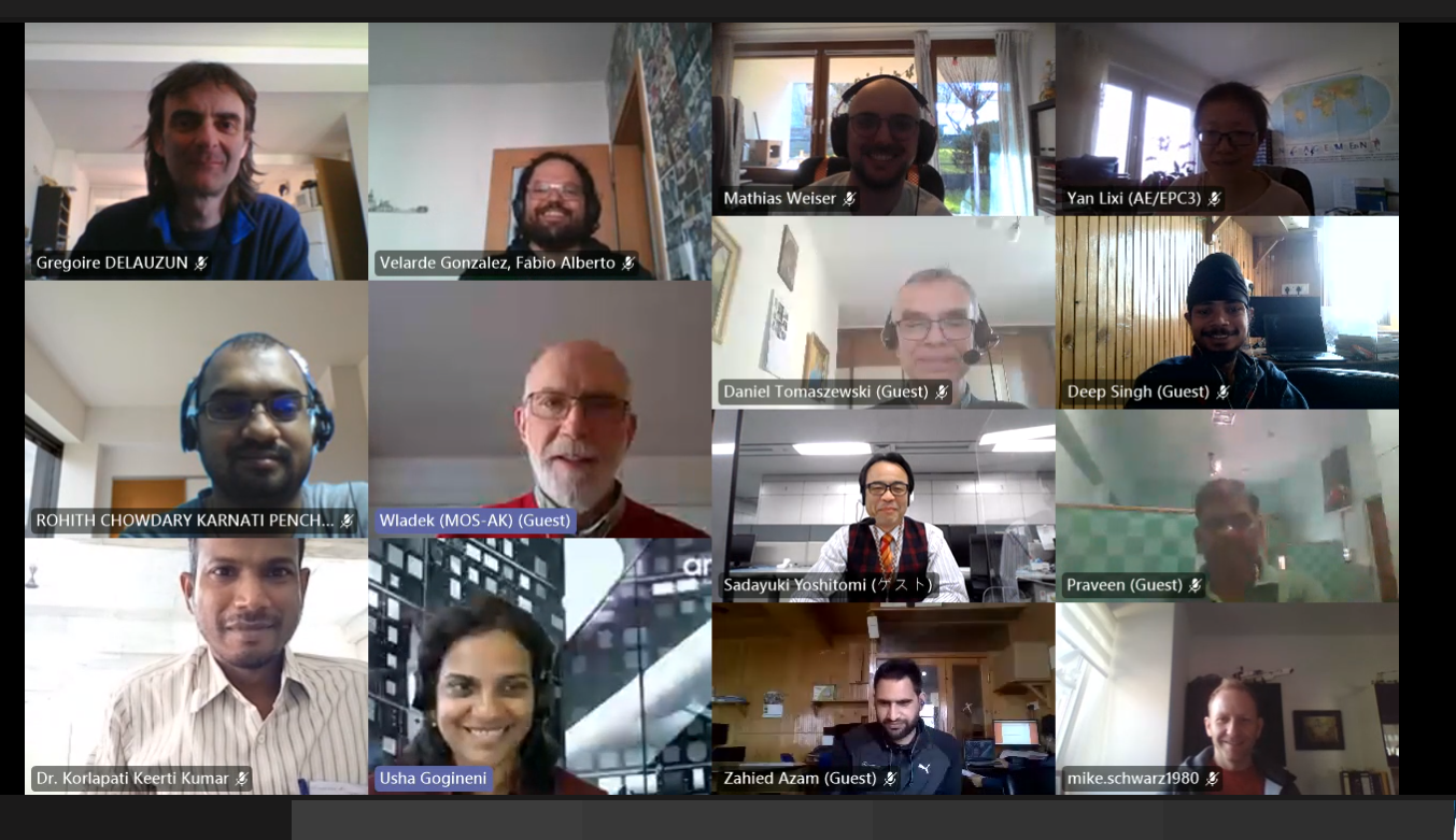
    Photo: All the MOS-AK/India Conference participants at IIT Hyderabad
    The MOS-AK Association plans to continue its standardization efforts by organizing future compact modeling meetings, workshops and courses arround the globe thru 2019 year, including:
    About MOS-AK Association:
    MOS-AK, an international compact modeling association primarily focused in Europe, to enable international compact modeling R&D exchange in the North/Latin Americas, EMEA and Asia/Pacific Regions. The MOS-AK Modeling Working Group plays a central role in developing a common information exchange system among foundries, CAD vendors, IC designers and model developers by contributing and promoting different elements of compact/SPICE modeling and its Verilog-A standardization and related CAD/EDA tools including FOSS for the compact/SPICE models development, validation/implementation and distribution. For more information please visit: mos-ak.org

    Tutorials:
    [1] Dr. Charvaka Duvvury iT2 Technologies (USA) ESD on-chip protection design 
    [2] Dr. Wladek Grabinski MOS-AK (EU) Verilog-A Standardization
    [3] Weronika Zubrzycka, AGH, (PL) Radiation effect and Radiation hardening in devices 
    [4] Prof. Roberto Murphy, INOE (MX) Characterization of Semiconductor Devices in the High Frequency Regime
    Keynote Talks: 
    [5] Prof. Yogesh Singh Chauhan, IIT Kanpur (IN) Negative Capacitance Transistors - Modeling, Simulation and Processor Performance
    [6] Dr. Surinder Singh, Semiconductor Labs, Chandigarh  (IN), Chandigarh Research at SCL
    [7] Weronika Zubrazycka, AGH, (PL) Radiation Effects on Circuits for Space and High-Energy Physics Applications - A case study 
    [8] Madabusi Govindrajan, GLOBALFOUNDRIES, Bangalore (IN)  Challenges for RF modeling in the connected era 
    [9] Dr. Usha Gogineni, Maxim Semiconductors (IN)  Compact Models for Analog and Mixed Signal Design 
    [10] Prof. Santanu Mahapatra, IISc, Bangalore (IN)  Atom-to-Circuit modeling technique for emerging nanomaterial based MOSFETs 
    [11] Prof. Gilson Wirth, UFRGS (BR) (Webinar) Charge Trapping Phenomena in MOSFETS: From Noise to Bias Temperature Instability 
    Plenary Talks: 
    [12] Prof. Jaijeet Roychowdhury, UC, Berkeley, USA Well-Posed Compact Modeling 
    [13] Dr. Ehrenfried Seebacher, ams (A) Compact Modeling for Industrial Applications 
    Panel Discussion: 
    [14] Dr. G. Uma Devi, Director, NRSC, (IN): Challenges and opportunities for Women in Engineering (WIE). 
    Best papers awards:
    [15] Chithra and Nagendra Krishnapura, "Modeling Techniques for Faster Verification of a Time to Digital Converter System-on-Chip Design"
    [16] Mohit Ganeriwala, Enrique Marin, Francisco Ruiz and Nihar Mohapatra," A Compact Charge and Surface Potential Model for III-V Quadruple-Gate FETs With Square Geometry"
    [17] Suprava Dey, Tara Prasanna Dash, Chinmay Kumar Maiti, Jhansirani Jena, Eleena Mohapatra and Sanghamitra Das," Performance Evaluation of Gate-All-Around Si Nanowire Transistors with SiGe Strain engineering"
    Headlines: 
    [18] "Swiss interest in India's energy and tech fields" Date: Feb. 27,2019 Publication: The Hindu Edition: Hyderabad
    [19] "IIT Hyderabad hosts MOS-AK India 2019 International Conference on Modeling of Systems Circuits and Devices" India Education diary  Edition: Online: Prof. Sushmee Badhulika 
    [19] Indo-Swiss collaboration needed in education" Date: Feb. 27,2019 Publication: The New Indian express, Edition: Hyderabad
    [20] "Switzerland looking forward to stronger ties with Telangana" Feb. 27,2019   Publication: Telangana Today, Edition:  Hyderabad
    [21] "IIT Hyderabad hosts MOS-AK India 2019 International Conference on Modeling of Systems Circuits and Devices " Date: Feb. 27,2019 Publication: Andhra Jyothi Edition: Hyderabad pp:3

    WG14032019

    --
    You received this message because you are subscribed to the Google Groups "mos-ak" group.
    To unsubscribe from this group and stop receiving emails from it, send an email to mos-ak+unsubscribe@googlegroups.com.
    To post to this group, send email to mos-ak@googlegroups.com.
    Visit this group at https://groups.google.com/group/mos-ak.
    For more options, visit https://groups.google.com/d/optout.

    Dec 21, 2018

    [mos-ak] [press note] 11th International MOS-AK Workshop, Silicon Valley, December 5, 2018

    Modeling of Systems and Parameter Extraction Working Group
    11th International MOS-AK Workshop
    Silvaco Inc. Headquarters, Silicon Valley, December 5, 2018
    Summary

    The MOS-AK Compact Modeling Association, a global standardization forum for semiconductor device models, held its 11th MOS-AK Workshop at the Silvaco Inc. headquarters in Santa Clara, Calif. on December 5, 2018. The event was co-located with the 2018 IEEE International Electron Devices (IEDM) and the Q4 Compact Modeling Coalition (CMC) meetings. The workshop receives technical program co-sponsorship from the IEEE Santa Clara Valley-San Francisco Chapter of the Electron Devices Society, Europractice, IJHSES as well as NEEDS of nanoHUB.org.

    Bogdan Tudor, Silvaco Inc. and Wladek Grabinski, MOS-AK, welcomed more than 30 international academic researchers and modeling engineers. The nine technical compact modeling presentations covered nanoscale technologies, semiconductor devices modeling and advanced IC design.

    The MOS-AK speakers shared their latest perspectives on compact/SPICE modeling and Verilog-A standardization in response to the dynamically evolving semiconductor industry and academic R&D efforts. The event featured advanced technical presentations covering compact model development, implementation, and deployment. For more information about each of the presentations, including full abstracts, go online to MOS-AK Workshop Silicon Valley 2018.

    The nine topics presented were the following:
    1. Silvaco GaN HEMT Compact Modeling Perspective, Bogdan Tudor, Colin Shaw and Sungwon Kong, Silvaco, Inc.
    2. GaN HEMT Devices and Modeling for Operational Electronics at Harsh Environments, Saleh Kargarrazi, XLab, Stanford University
    3. Impact of Basal Plane Dislocations and Ruggedness of 10 kV 4H-SiC Transistors, Victor Veliadis, PowerAmerica, North Carolina State University
    4. Direct measurement of white noise in MOSFETs, Kenji Ohmori, Device Lab Inc.
    5. NEREID Technology Roadmap, Enrico Sangiorgi, NEREID, University of Bologna
    6. A Physics-Based Compact Model of RRAM for Emerging Applications, Paolo Pavan, University of Modena and Reggio Emilia
    7. From Physics to Power, Performance, and Parasitics, Oskar Baumgartner, Global TCAD Solutions GmbH
    8. MOS-AK FOSS Compact Modeling Perspective, Wladek Grabinski, IEEE EDS DL, MOS-AK
    9. Compact Model of Single TeraFET Spectrometer, Michael Shur, Rensselaer Polytechnic Institute
    There were also presentations of Late News with the following topics:
    1. CMC Developer Model Software Licenses, Peter Lee, Micron
    2. Xyce Parallel Electronic Simulator (Ver. 6.10), Jason Verley, Sandia National Laboratories
    3. Call for Papers for ESSDERC/ESSCIRC 2019 in Krakow, Wladek Grabinski, MOS-AK
    Photo: Some of the participants of the 11th MOS-AK Workshop at Silvaco Inc. Headquarters in Silicon Valley.

    The MOS-AK Association plans to continue its standardization efforts by organizing future compact modeling meetings, workshops and courses in India, China, Europe, USA and, for the very first time, in Latin America, throughout the coming year, including:
    About Silvaco:
    Silvaco, Inc. is a leading EDA tools and semiconductor IP provider used for process and device development for advanced semiconductors, power IC, display and memory design. For over 30 years, Silvaco has enabled its customers to develop next generation semiconductor products in the shortest time with reduced cost. We are a technology company outpacing the EDA industry by delivering innovative smart silicon solutions to meet the world's ever-growing demand for mobile intelligent computing. The company is headquartered in Santa Clara, California and has a global presence with offices located in North America, Europe, Japan and Asia.

    About Europractice IC Service:
    The EUROPRACTICE IC Service brings ASIC design and manufacturing capability within the technical and financial reach of any company that wishes to use ASICs. The EUROPRACTICE IC Service, offered by IMEC and Fraunhofer, offers low-cost ASIC prototyping and ASIC small volume production ramp-up to high volume production through Multi Project Wafer - MPW - and dedicated wafer runs.

    About MOS-AK Association:
    MOS-AK is an international compact modeling association primarily focused in Europe, to enable international compact modeling R&D exchange in the North/Latin Americas, EMEA and Asia/Pacific Regions. The MOS-AK Modeling Working Group plays a central role in developing a common information exchange system among foundries, CAD vendors, IC designers and model developers by contributing and promoting different elements of compact/SPICE modeling and its Verilog-A standardization and related CAD/EDA tools including FOSS for compact/SPICE model development, validation/implementation and distribution. For more information please visit mos-ak.org

    Oct 19, 2016

    [mos-ak] [2nd Announcement and Call for Papers] 9th International MOS-AK Workshop Berkeley DEC.7, 2016

     9th International MOS-AK Workshop  
      Berkeley December 7, 2016 
        2nd Announcement and Call for Papers   

    Together with the MOS-AK workshop host, Prof. Jaijeet Roychowdhury, UCB and International MOS-AK Board of R&D Advisers: Larry Nagel, Omega Enterprises Consulting (USA), Andrei Vladimirescu, UCB (USA); ISEP (FR) as well as all the Extended MOS-AK TPC Committee, we have pleasure to invite to the 9th International MOS-AK Workshop which will be held at EECS Department, University of California, Berkeley on December, 7, 2016. Planned MOS-AK workshop is organized with aims to strengthen a network and discussion forum among experts in the field, enhance open platform for information exchange related to compact/SPICE modeling and Verilog-A standardization, bring people in the compact modeling field together, as well as obtain feedback from technology developers, circuit designers, and CAD/EDA tool developers and vendors.

    Important Dates:
    • Preannouncement - Sept 2016
    • Call for Papers - Oct. 2016
    • Final Workshop Program - Nov. 2016
    • MOS-AK Workshop - Dec. 7 2016
    Venue:
    EECS Department
    University of California, Berkeley

    Topics to be covered include the following among other related to the compact/SPICE modeling :
    • Compact Modeling (CM) of the electron devices
    • Advances in semiconductor technologies and processing
    • Verilog-A language for CM standardization
    • New CM techniques and extraction software
    • Open Source TCAD/EDA modeling and simulation
    • CM of passive, active, sensors and actuators
    • Emerging Devices, TFT, CMOS and SOI-based memory cells
    • Microwave, RF device modeling, high voltage device modeling
    • Nanoscale CMOS devices and circuits
    • Technology R&D, DFY, DFT and reliability/ageing IC Designs
    • Foundry/Fabless Interface Strategies
    Online MOS-AK Abstract Submission:
    Prospective authors should submit online 
    (any related inquiries can be sent to abstracts@mos-ak.org)

    Online Workshop Registration:
    http://www.mos-ak.org/berkeley_2016/registration.php
    (any related inquiries can be sent to register@mos-ak.org)

    Postworkshop Publications:
    Selected best MOS-AK technical presentation will be recommended for further publication in a special issue of the International Journal of High Speed Electronics and Systems

    Extended MOS-AK Committee

    WG19102016
    --
    You received this message because you are subscribed to the Google Groups "mos-ak" group.
    To unsubscribe from this group and stop receiving emails from it, send an email to mos-ak+unsubscribe@googlegroups.com.
    To post to this group, send email to mos-ak@googlegroups.com.
    Visit this group at https://groups.google.com/group/mos-ak.
    For more options, visit https://groups.google.com/d/optout.