Showing posts with label ekv. Show all posts

Apr 15, 2024

[course] MEAD @ EPFL

Live Course @ EPFL, Lausanne, Switzerland
JUNE 17-21, 2024

Registration Deadline: May 17, 2024 >> REGISTER

MONDAY, June 17

8:30 am-12:00 pmMOS Transistor Modeling for Low-Voltage and Low-Power Circuit DesignChristian Enz
1:30-5:00 pmDesign of Low-Power Analog Circuits using the Inversion CoefficientChristian Enz

TUESDAY, June 18

8:30 am-12:00 pmNoise Performance of Elementary Circuit BlocksBoris Murmann
1:30-5:00 pmOpamp Topologies and Design FundamentalsBoris Murmann

WEDNESDAY, June 19

8:30-10:00 amLow-Power High Efficiency OpAmp DesignKlaas Bult
10:30 am-12:00 pmLow-Power High Efficiency Residue AmplifiersKlaas Bult
1:30-3:00 pmAnalog Design Methodology and Practical Techniques for Frequency CompensationVadim Ivanov
3:30-5:00 pmEnergy Efficient Voltage References, Biasing in Analog Systems and Current SourcesVadim Ivanov

THURSDAY, June 20

8:30-10:00 amPower Dissipation in ADC Buidling BlocksKlaas Bult
10:30 am-12:00 pmPower Dissipation in ADCsKlaas Bult
1:30-5:00 pmMicropower ADCsKofi Makinwa

FRIDAY, June 21

8:30 am-12:00 pmEnergy Efficient Sensor InterfacesTaekwang Jang
1:30-5:00 pmLow-Power Frequency Reference CircuitsTaekwang Jang
1:30-5:00 pmPower Management With Nanoampere Consumption and Efficient Energy HarvestingVadim Ivanov

Nov 29, 2023

[paper] Noise modeling for cryogenic applications

Giovani Britton1,2, Salvador Mir2, Estelle Lauga-Larroze2, Benjamin Dormieu1, Quentin Berlingard3,4, Mickael Casse3 and Philippe Galy1
Noise modeling using look-up tables and DC measurements for cryogenic applications.
VLSI-SoC 2023 - 31st IFIP/IEEE International Conference on Very Large Scale Integration,
Oct 2023, Sharjah, United Arab Emirates.
DOI: 10.1109/VLSI-SoC57769.2023.10321896
hal-04305746
1STMicroelectronics, Crolles, France
2Univ. Grenoble Alpes, CNRS, Grenoble-INP, TIMA
3Univ. Grenoble Alpes, CEA, LETI
4Univ. Grenoble Alpes, CNRS, Grenoble-INP, IMEP-LAHC

Abstract : There is today a lack of mature transistor-level compact models for the simulation of integrated circuits at cryogenic temperatures. This is particularly the case for the simulation of the noise behavior which is critical for most applications. In this paper, we aim at an efficient prediction of the white noise behavior of basic amplifying stages working at RF frequencies and cryogenic temperatures. For this, we propose the use of DC measurements that are incorporated in a LookUp Table (LUT) and fed to a mathematical noise model. We illustrate the approach for the case of a transistor in common source configuration. The results of circuit simulation of the noise parameters in the standard temperature range are very close to the estimation of the same parameters using the LUT with just DC measurements. The approach can be readily extended to the analysis of circuits with multiple components. Next, the LUT approach is used for estimating the noise parameters at cryogenic conditions, considering DC measurements that have been carried out at these temperatures. The paper illustrates the feasibility of carrying out a cryogenic design using a LUT-based approach while accurate compact models are not yet available.

Fig : Measurement data and EKV or ACM generated parameters are added
to the LUT generated by the interface between EDA tools

Acknowledgments : This work was supported by the French program Conventions Industrielles de Formation par la Recherche (CIFRE) and Labex MINOS of French program ANR-10-LABX-55-01.

Mar 15, 2023

[paper] highly segmented hybrid pixel detectors

R. Ballabrigaa, J.A. Alozya, F.N. Bandia, G. Blajb, M. Campbella, P. Christodouloua c d, V. Cocoa, A. Dordaa e, S. Emiliania h, K. Heijhoff f, E. Heijne a c, T. Hofmanna, J. Kaplona, A. Koukabh,
I. Kremastiotisa, X. Lloparta, M. Noya, A. Paternoa, M. Pillera g, J.M. Sallesseh, V. Sriskarana,
L. Tlustosa c, M. van Beuzekomf
The Timepix4 analog front-end design: Lessons learnt on fundamental limits to noise and time resolution in highly segmented hybrid pixel detectors
Research Section A: Accelerators, Spectrometers, Detectors and Associated Equipment
Volume 1045, 1 January 2023, 167489
DOI: 10.1016/j.nima.2022.167489

a CERN, Experimental Physics Department, Meyrin, 1211, Switzerland
b SLAC National Accelerator Laboratory, Menlo Park, 94025, CA, United States
c IEAP, Czech Technical University in Prague, Prague, 11000, Czech Republic
d Department of Biomedical technology, Faculty of Biomedical Engineering, Czech Technical University in Prague, nam. Sitna 3105, Kladno, 272 01, Czech Republic
e KIT - Karlsruhe Institute of Technology, Institute for Data Processing and Electronics (IPE), Hermann-von-Helmholtz-Platz 1, Eggenstein-Leopoldshafen, 76344, Germany
f Nikhef, Science Park 105, Amsterdam, 1098, Netherlands
g Institute of Electronics, Graz University of Technology, Graz, 8010, Austria
h Electron Device Modeling and Technology Laboratory (EDLAB), EPFL, Switzerland


Abstract: This manuscript describes the optimization of the front-end readout electronics for high granularity hybrid pixel detectors. The theoretical study aims at minimizing the noise and jitter. The model presented here is validated with both circuit post layout simulations and measurements on the Timepix4 Application Specific Integrated Circuit (ASIC). The analog front-end circuit and the procedure to optimize the dimensions of the main transistors are described with detail. The Timepix4 is the most recent ASIC designed in the framework of the Medipix4 Collaboration. It was manufactured in 65 nm CMOS process, and consists of a four side buttable matrix of 448X512 pixels with 55µm pitch. The analog front-end has a gain of 36 mV/ke- when configured in High Gain Mode, and 20 mV/ke- when configured in Low Gain Mode. The Equivalent Noise Charge (ENC) is ~68e-rms and ~80e-rms in High Gain Mode and in Low Gain Mode respectively. In event driven mode, the incoming hits can be time stamped within a 200ps time bin and the chip can deal with a maximum flux of 3.6MHz mm-2s-1. In photon counting mode, the chip can deal with up to 5GHz mm-2s-1. The routine designed to optimize the Timepix4 front-end is then used to analyze the performance limits in terms of jitter and noise for Charge Sensitive Amplifiers in pixel detectors.

Fig: Transconductance that can be obtained for the input transistor as an EKV function of the Inversion Coefficient (IC). The asymptotes for the velocity without and with velocity saturation are shown.

Acknowledgments: The authors would like to acknowledge the Medipix Collaborations for their continuous support in the design of hybrid pixel detector readout chips.

May 13, 2022

[Presentation] reached 200 reads on RG


Yogesh S. Chauhan; Muhammed Karim (Rumi); Sriram V.; Sourabh Khandelwal; Ali Niknejad; Chenming Hu; Weimin Wu; Krishnanshu Dandu; Keith Green; Geoffrey Coram; Sergey Cherepko; Jing Wang; Saurabh Sirohi; Josef Watts; Maria-Anna Chalkiadaki; Anurag Mangla; Antonios Bazigos; Francois Krummenacher; Wladek Grabinski; Christian Enz;
presented at the Nano-Tera Workshop (EPFL Nano-Tera),
Lausanne, Dec. 15, 2011
doi: 10.5281/zenodo.6546258.

Outline: BSIM6 is the next BSIM Bulk MOSFET model
  • Charge based core derived from Poisson's solution
  • Physical effects (SCE, CLM etc.) taken from BSIM4
  • Parameter names matched to BSIM4 parameters
  • Gummel Symmetry (symmetric @ VDS=0)
FIG: Gummel Symmetry (symmetric @ VDS=0)


Oct 26, 2021

conference paper reached 400 reads

conference paper reached 400 reads

Bucher, M., J-M. Sallese, F. Krummenacher, D. Kazazis, C. Lallement, W. Grabinski, and C. Enz
EKV 3.0: An analog design-oriented MOS transistor model
In 9th International Conference on Mixed Design of Integrated Circuits and Systems
(MIXDES 2002)

Abstract:  The EKV 3.0 compact MOS transistor model for advanced analog IC design and simulation is presented. The model is based on the surface potential approach combined with inversion charge linearization. The ideal long-channel model is coherent  for  static  and  dynamic  aspects  including  noise.  The  ideal  model  is  extended  for  high-field  effects  in  deep submicron CMOS technologies. Scalability over channel length and width is achieved while retaining a reduced number of parameters. The EKV 3.0 model is applicable over a large range of CMOS technologies.  

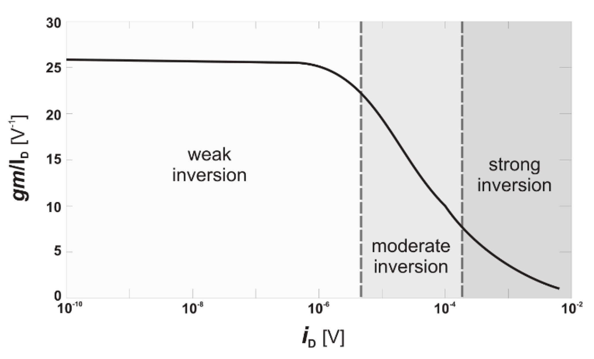
Fig: Normalized source transconductance to current ratio (gm/ID) vs. normalized current, measured 
(markers) in saturation from various CMOS technologies, and analytical model.


Oct 21, 2021

[paper] Charge-based Modeling of FETs

Jean-Michel Sallese 
Charge-based modeling of field effect transistors, Make it easy
Joint International EUROSOI and EuroSOI-ULIS Workshop (Sept.2020)
DOI: 10.1109/EuroSOI-ULIS53016.2021.956068
 
EDLab, EPFL,  Lausanne  (CH)
 
Abstract: In this presentation, we revisit some charge voltage dependencies for different architectures of field effect transistor, emphasizing on compactness and simplicity while maintaining a close link with physics, which makes these models predictive and accurate for general purposes of compact modeling.

Fig: The gm/I invariant versus the inversion coefficient IC. 
The operation modes of the MOSFET are clearly defined. 

Acknowledgements: I (JMS) would like to thank F. Jazaeri, C. Lallement, W. Grabinski, B. Iniguez and M. Bucher for their constructive interactions. 


Sep 17, 2021

[paper] EKV Model for Bulk-Driven Circuit Design Using gmb/ID Method

Lukas Nagy, Daniel Arbet, Martin Kovac, Miroslav Potocny, Robert Ondica and Viera Stopjakova
EKV Model for Bulk-Driven Circuit Design Using gmb/ID Method
IEEE AFRICON; 13-15 September 2021; Arusha (TZ)
 
Institute of Electronics and Photonics; Faculty of Electrical Engineering and Information Technology; Slovak University of Technology; Bratislava (SK)

Abstract: The paper addresses a development and application of EKV MOS transistor compact model with focus on the ultra low-voltage / ultra low-power analog integrated circuit (IC) design employing bulk-driven (BD) technique. The presented contribution can be viewed as an extension of standard EKV model application and as a contribution to ultra low-voltage IC design techniques. The paper compares the measured and extracted small-signal parameters of standalone transistor samples fabricated in 130 nm CMOS technology and the simulation results obtained using the proposed bulk-driven EKV v2.63 model and foundry-provided BSIM model v3.3. The transistor samples were analyzed with power supply of VDD = 0.4 V The paper also discusses the implementation of 3D graphs as a result of introducing another degree of freedom into the essential MOS transistor characteristics, while maintaining the ease of using the design hand-calculation with the original gm/ID approach.

Fig: Bulk-Driven TEF vs Inversion Coefficient – gmb/ID

Acknowledgment: This work has been supported in part by the Slovak Research and Development Agency under grant APVV 19-0392, the Ministry of Education, Science, Research and Sport of the Slovak Republic under grants VEGA 1/0731/20 and VEGA 1/0760/21, and ECSEL JU under project PROGRESSUS (Agr. No. 876868)

Aug 30, 2021

Generalized EKV Compact MOSFET Model

On the Explicit Saturation Drain Current in the Generalized EKV Compact MOSFET Model
Francisco J. García-Sánchez, Life Senior Member, IEEE,
and Adelmo Ortiz-Conde, Senior Member, IEEE
IEEE TED Aug 9. 2021
DOI: 10.1109/TED.2021.3101186

*Solid State Electronics Laboratory, Universidad Simón Bolívar, Caracas 1080, Venezuela


Abstract: We present and discuss explicit closed-form expressions for the saturation drain current of short channel metal-oxide-semiconductorfield-effect transistors (MOSFETs) with gate oxide and interface-trapped charges, and including carrier velocity saturation, according to the generalized Enz-Krummenacher-Vittoz (EKV) MOSFET compact model. The normalized saturation drain current is derived as an explicit function of the normalized terminal voltages by solving the transcendental voltage versus charge equation using the Lambert W function. Because this special function is analytically differentiable, other important quantities, such as the transconductance and the transconductance-to-currentratio, can be readily expressed as explicit functions of the terminal voltages.
Fig: Comparison of simulated transfer characteristics with (red lines and symbols) and another without (black lines and symbols) radiation-induced oxide and interface-trapped charges. Calculation of VGB versus IDsat (lines) comes from denormalization and the explicit IDsat versus VGB (symbols) comes from denormalization of the proposed explicit expressions


Apr 19, 2021

[paper] Deep-Learning Assisted Compact Modeling

Hei Kam
Deep-Learning Assisted Compact Modeling of Nanoscale Transistor
CS230 Deep Learning; Stanford University (2021)

Abstract - Transistors are the basic building blocks for all electronics. Accurate prediction of their current-voltage (IV) characteristics enables circuit simulations before the expensive silicon tape-out. In this work, we propose using deep neural network to improve the accuracy for the conventional, physics-based compact model for nanoscale transistors. Physics-driven requirements on the neural network are discussed. Using finite element simulation as the input dataset, together with a neural network with roughly 30 neurons, the final IV model can well-predict the IV to within 1%. This modelling methodologies can be extended for other transistor properties such as capacitance-voltage (CV) characteristics, and the trained model can readily be implemented by the hardware description language (HDL) such as Verilog-A for circuit simulation. The EKV model [1-2] is used as an example. Other transistor models such as BSIM-MG [3] or PSP [4] model can also be used.

Fig: Architecture for the 3-layer neural network together with the aforementioned transformation T. Hyperbolic tangent function tanh(x) is used as the activation function for the input and hidden layers due to its infinite differentiability.

References:
[1] Enz, Christian C., Eric A. Vittoz; "Charge-based MOS transistor modeling." John Wiely & Sons Inc 68 (2006).
[2] FOSS EKV 2.6 Compact Model <https://github.com/ekv26/model>
[3] Khandelwal, Sourabh, et al. "BSIM-IMG: A compact model for ultrathin-body SOI MOSFETs with back-gate control." IEEE Transactions on Electron Devices 59.8 (2012): 2019-2026.
[4] Gildenblat, G., et al. "PSP Model." Department of Electrical Engineering, The Pennsylvania State University and Philips Research, (Aug. 2005)

Jan 7, 2021

[paper] Generalized EKV Charge-based MOSFET Model

A Generalized EKV Charge-based MOSFET Model Including Oxide and Interface Traps
Chun-Min Zhanga,  Farzan Jazaeria,  Giulio Borghellob,  Serena Mattiazzoc,  Andrea Baschirottod
and Christian Enza
Available online 7 January 2021, 107951
Open Access under a Creative Commons License
DOI: 10.1016/j.sse.2020.107951

a Integrated Circuits Laboratory (ICLAB), École Polytechnique Fédérale de Lausanne (EPFL), Neuchâtel 2000, Switzerland
b Department of Experimental Physics, CERN, Geneva 1211, Switzerland
c Department of Information Engineering, INFN Padova and University of Padova, Padova 35131, Italy
d Microelectronic Group, INFN Milano-Bicocca and University of Milano-Bicocca, Milano 20126, Italy

Abstract: This paper presents a generalized charge-based EKV MOSFET model that includes the effects of trapped charges in the bulk oxide and at the silicon/oxide interface. It is shown that in the presence of oxide- and interface-trapped charges, the mobile charge density can still be linearized but with respect to both the surface potential and the channel voltage. This enables us to derive closed-form expressions for the mobile charge density and the drain current. These simple formulations demonstrate the effects of charge trapping on MOSFET characteristics and crucial device parameters. The proposed charge-based analytical model, including the effect of velocity saturation, is successfully validated through measurements performed on devices from a 28nm bulk CMOS technology. Ultrahigh total ionizing doses up to 1 Grad (SiO2) are applied to generate oxide-trapped charges and activate the passivated interface traps. Despite a small number of parameters, the model is capable of accurately capturing the measurement results over a wide range of device operation from weak to strong inversion. Explicit expressions of device parameters also allow for the extraction of the oxide- and interface-trapped charge density.

Fig: Energy band diagrams illustrating interface charge trapping in bulk n- (a) and pMOSFETs (b) in inversion. The quasi-Fermi level of the minority carriers, 𝐸𝐹𝑛 or 𝐸𝐹𝑝, is split from that of the majority carriers 𝐸𝐹 by the channel voltage 𝑉𝑐ℎ

Acknowledgements: The authors would like to thank the EP-ESE group at CERN, especially Dr. Federico Faccio, for the continuous support in radiation measurements and the interesting discussions about data analysis. This work was supported in part by the Swiss National Science Foundation (SNSF) through the GigaradMOST project under grant number 200021_160185 and in part by the Istituto Nazionale di Fisica Nucleare (INFN) through the ScalTech28 Project.

Sep 9, 2020

[paper] Analogue 2D Semiconductor Electronics

Analogue two-dimensional semiconductor electronics
Dmitry K. Polyushkin1, Stefan Wachter1, Lukas Mennel1, Matthias Paur1, Maksym Paliy2, Giuseppe Iannaccone2, Gianluca Fiori2, Daniel Neumaier3,4, Barbara Canto3,4
and Thomas Mueller1
Nat Electron 3, 486–491 (2020)
DOI: 10.1038/s41928-020-0460-6

1Vienna University of Technology, Institute of Photonics, Vienna, Austria. 
2Dipartimento di Ingegneria dell’Informazione, Università di Pisa, Pisa, Italy.
3AMO GmbH, Aachen, Germany. 
4Bergische Universität Wuppertal, Wuppertal, Germany

Abstract: Digital electronics are ubiquitous in the modern world, but analogue electronics also play a crucial role in many devices and applications. Analogue circuits are typically manufactured using silicon as the active material. However, the desire for improved performance, new devices and flexible integration has—as for their digital counterparts—led to research into alternative materials, including the use of two-dimensional (2D) materials. Here, we show that operational amplifiers—a basic building block of analogue electronics—can be created using the 2D semiconductor molybdenum disulfide (MoS2) as the active material. The device is capable of stable operation with good performance, and we demonstrate its use in feedback circuits including inverting amplifiers, integrators, log amplifiers and transimpedance amplifiers. We also show that our 2D platform can be used to monolithically integrate an analogue signal preconditioning circuit with a MoS2 photodetector.

Fig: a) Schematic of the back-gated transistor architecture; 
b) Transfer characteristics of a typical transistor on the chip (W/L = 4); 
c) View of a single OPA showing the pinout and transistor labelling

Circuit design and modelling: Because a complete model of back-gated 2D semiconductor FETs is still not readily available, we fitted the experimental results with an Enz–Krummenacher– Vittoz (EKV) model in both, the subthreshold and inversion, regimes. All the transistors operate in the inversion regime, we used the inversion model to simulate the OPA, obtaining a nominal low-frequency Atot gain value.

Acknowledgements: We thank A.J. Molina-Mendoza for technical assistance and N. Schaefer and J.A. Garrido for providing a polyimide substrate. We acknowledge financial support by the European Union (grant agreements 785219 Graphene Flagship, 796388 ECOMAT and 828901 ORIGENAL), the Austrian Science Fund FWF (START Y 539-N16) and the Italian MIUR (FIVE 2D).

May 18, 2020

[paper] Novel Design and Optimization and the gm/ID Ratio

A Novel Design and Optimization Approach for Low Noise Amplifiers (LNA) Based on MOST Scattering Parameters and the gm/ID Ratio
1Facultad de Ingeniería, Universidad Católica de Córdoba, Córdoba 5017 (AN)
2Service d’Électronique et Microélectronique, Université de Mons (UMONS), 7000 Mons (BE)
3Departamento de Electrónica, Instituto de Astrofísica de Canarias (IAC), 38200 La Laguna (SP)
* Author to whom correspondence should be addressed.
Electronics 2020, 9(5), 785; https://doi.org/10.3390/electronics9050785
Received: 31 March 2020 / Revised: 30 April 2020 
Accepted: 9 May 2020 / Published: 11 May 2020

AbstractThis work presents a new design methodology for radio frequency (RF) integrated circuits based on a unified analysis of the scattering parameters of the circuit and the gm/ID ratio of the involved transistors. Since the scattering parameters of the circuits are parameterized by means of the physical characteristics of transistors, designers can optimize transistor size and biasing to comply with the circuit specifications given in terms of S-parameters. A complete design of a cascode low noise amplifier (LNA) in 65nm CMOS technology is taken as a case study in order to validate the approach. In addition, this methodology permits the identification of the best trade-off between the minimum noise figure and the maximum gain for the LNA in a very simple way.
Figure: gm/ID versus iD

Acknowledgement - This research was funded by Universidad Católica de Córdoba (Argentina), the Walloon Region DGO6 BEWARE Fellowships Academia Programme (1410164-POHAR, cofunded by the European Marie Curie Actions), the Belgian FNRS (Fond National pour la Recherche Scientifique) and the Argentinean MINCyT (Ministerio de Ciencia y Tecnología).

Feb 8, 2018

BSIM3v3 to EKV2.6 Model Parameter Extraction

BSIM3v3 to EKV2.6 Model Parameter Extraction and Optimisation
using LM Algorithm on 0.18um Technology node
Kirmender Singh and Piyush Jain
Int. Journal of Electronics and Telecommunications 2018 Vol.64 No.1 pp.5-11

Abstract: The industry standard BSIM3v3 and BSIM4.0 have been replaced by BSIM6.0 compact MOSFET model for deep submicron technology node. The BSIM6.0 is next generation, defacto industry standard model for bulk MOSFET. This model is charge based which is continuous from weak to strong inversion of operation. The core of analytical and physical BSIM6 model[3] is charge, with drain current equation expressed in form of source (qs) and drain charge (qd). This model has all its governing equations continuous and can be used to develop design methodology using IC based approach. But its method of computing qs and qd is complicated which is different from Vittoz traditional charge calculation method. The continuous interpolation equation of drain current as adopted by EKV2.6 although is empirical but its compact expression is preferred by analog designer to get intuitive design guidance. BSIM6 is a combined effort by BSIM and EKV modeling groups based on charge based continuous equations. Although EKV2.6 model is not valid for deep submicron process as it only includes submicron short channel effects like velocity saturation (VS), vertical field mobility reduction (VFMR), Drain induced barrier lowering (DIBL), channel length modulation (CLM) etc. But it still offers some benefits to have first cut design methodology because of its much simplified analytical equations. The inversion coefficient (IC) has found extensive acceptance in designer community as it offers enhanced design elegance in EKV then more complicated BSIM model. This paper discuses first step in analog design process by extracted core EKV2.6 intrinsic model parameters from industry standard BSIM3v3 model on 0.18µ technology node. The 0.18µ technology is chosen as it is still more common technology node in analog circuit design. The model parameters are extracted for different bins and optimisation is done using nonlinear optimisation LM algorithm. The optimised EKV2.6 parameters are validated with currentvoltage(I-V), intrinsic voltage gain (Avi) and Early voltage circuit parameter (VA) with BSIM3v3 model [read more...]

Flow-chart of BSIM to EKV conversion steps
(source:
D. Stefanovic and M. Kayal “Structured Analog CMOS Design" Springer Publications, 2008)

Oct 24, 2017

Cryogenic characterization of CMOS technologies

A. Beckers, F. Jazaeri, A. Ruffino, C. Bruschini, A. Baschirotto and C. Enz
Cryogenic characterization of 28 nm bulk CMOS technology for quantum computing
47th ESSDERC, Leuven, Belgium, 2017, pp. 62-65.

Abstract: This paper presents the first experimental investigation and physical discussion of the cryogenic behavior of a commercial 28 nm bulk CMOS technology. Here we extract the fundamental physical parameters of this technology at 300,77 and 4.2 K based on DC measurement results. The extracted values are then used to demonstrate the impact of cryogenic temperatures on the essential analog design parameters. We find that the simplified charge-based EKV model can accurately predict the cryogenic behavior. This represents a main step towards the design of analog/RF circuits integrated in an advanced bulk CMOS process and operating at cryogenic temperature for quantum computing control systems [read more...doi: 10.1109/ESSDERC.2017.8066592


R. M. Incandela, L. Song, H. A. R. Homulle, F. Sebastiano, E. Charbon and A. Vladimirescu
Nanometer CMOS characterization and compact modeling at deep-cryogenic temperatures
47th ESSDERC, Leuven, Belgium, 2017, pp. 58-61.

Abstract: The characterization of nanometer CMOS transistors of different aspect ratios at deep-cryogenic temperatures (4 K and 100 mK) is presented for two standard CMOS technologies (40 nm and 160 nm). A detailed understanding of the device physics at those temperatures was developed and captured in an augmented MOS11/PSP model. The accuracy of the proposed model is demonstrated by matching simulations and measurements for DC and time-domain at 4 K and, for the first time, at 100 mK [read more...doi: 10.1109/ESSDERC.2017.8066591

Sep 12, 2017

[book] Systematic Design of Analog CMOS Circuits

Paul G. A. Jespers, Boris Murmann
Cambridge University Press; 31 Oct 2017; 342pp

Discover a fresh approach to efficient and insight-driven analog integrated circuit design in nanoscale-CMOS with this hands-on guide. Expert authors present a sizing methodology that employs SPICE-generated lookup tables, enabling close agreement between hand analysis and simulation. This enables the exploration of analog circuit tradeoffs using the gm/ID ratio as a central variable in script-based design flows, and eliminates time-consuming iterations in a circuit simulator. Supported by downloadable MATLAB code, and including over forty detailed worked examples, this book will provide professional analog circuit designers, researchers, and graduate students with the theoretical know-how and practical tools needed to acquire a systematic and re-use oriented design style for analog integrated circuits in modern CMOS.

Aug 28, 2017

[paper] Nanoscale MOSFET Modeling

 Nanoscale MOSFET Modeling: 
Part 1: The Simplified EKV Model for the Design of Low-Power Analog Circuits
C. Enz, F. Chicco and A. Pezzotta
in IEEE Solid-State Circuits Magazine, vol. 9, no. 3, pp. 26-35, Summer 2017
doi: 10.1109/MSSC.2017.2712318

Abstract: This article presents the simplified charge-based Enz-Krummenacher-Vittoz (EKV) [11] metal-oxide-semiconductor field-effect transistor (MOSFET) model and shows that it can be used for advanced complementary metal-oxide-semiconductor (CMOS) processes despite its very few parameters. The concept of an inversion coefficient (IC) is first introduced as an essential design parameter that replaces the overdrive voltage VG-VT0 and spans the entire range of operating points from weak via moderate to strong inversion (SI), including the effect of velocity saturation (VS). The simplified model in saturation is then presented and validated for different 40- and 28-nm bulk CMOS processes. A very simple expression of the normalized transconductance in saturation, valid from weak to SI and requiring only the VS parameter mc, is described. The normalized transconductance efficiency Gm/ID, which is a key figure-of-merit (FoM) for the design of low-power analog circuits, is then derived as a function of IC including the effect of VS. It is then successfully validated from weak to SI with data measured on a 40-nm and two 28-nm bulk CMOS processes. It is then shown that the normalized output conductance Gds/ID follows a similar dependence with IC than the normalized Gm/ID characteristic but with different parameters accounting for drain induced barrier lowering (DIBL). The methodology for extracting the few parameters from the measured ID-VG and ID-VD characteristics is then detailed. Finally, it is shown that the simplified EKV model can also be used for a fully depleted silicon on insulator (FDSOI) and Fin-FET 28-nm processes [read more...]

FIG: The simplified EKV model applied to a 28-nm FDSOI CMOS process: 
Gm n UT / ID versus IC for three different transistor channel lengths

References
[1] A. Bahai, “Ultra-low energy systems: Analog to information,” in Proc. European Solid-State Circ. Conf., Sept. 2016, pp. 3–6.
[2] D. Binkley, Tradeoffs and Optimization in Analog CMOS Design. Hoboken, NJ: Wiley, 2008.
[3] W. Sansen, Analog Design Essentials. New York: Springer-Verlag, 2006.
[4] A. Mangla, M. A. Chalkiadaki, F. Fadhuile, T. Taris, Y. Deval, and C. C. Enz, “Design methodology for ultra low-power analog circuits using next generation BSIM6 MOSFET compact model,” Microelectr. J., vol. 44, no. 7, pp. 570–575, July 2013.
[5] Y. S. Chauhan, S. Venugopalan, M. A. Chalkiadaki, M. A. U. Karim, H. Agarwal, S. Khandelwal, N. Paydavosi, J. P. Duarte, C. C. Enz, A. M. Niknejad, and C. Hu, “BSIM6: Analog and RF compact model for bulk MOSFET,” IEEE Trans. Electron Dev., vol. 61, no. 2, pp. 234–244, Feb. 2014.
[6] C. Enz, M. A. Chalkiadaki, and A. Mangla, “Low-power analog/RF circuit design based on the inversion coefficient,” in Proc. European Solid-State Circ. Conf., Sept. 2015, pp. 202–208.
[7] C. Enz and A. Pezzotta, “Nanoscale MOSFET modeling for the design of low-power analog and RF circuits,” in Proc. Int. Conf. MIXDES, June 2016, pp. 21–26.
[8] W. Sansen, “Analog CMOS from 5 micrometer to 5 nanometer,” in Proc. IEEE Int. Solid State Circuits Conf. Dig. Tech. Papers, Feb. 2015, pp. 1–6.
[9] W. Sansen, “Analog design procedures for channel lengths down to 20 nm,” in Proc. IEEE 20th Int. Conf. Electronics, Circuits, and Systems, Dec. 2013, pp. 337–340.
[10] C. C. Enz and E. A. Vittoz, Charge-Based MOS Transistor Modeling - The EKV Model for Low-Power and RF IC Design. Hoboken, NJ: Wiley, 2006.
[11] C. C. Enz, F. Krummenacher, and E. A. Vittoz, “An analytical MOS transistor model valid in all regions of operation and dedicated to low-voltage and low-current applications,” Analog Integr. Circuits Signal Process. J., vol. 8, pp. 83–114, July 1995.
[12] P. Heim, S. R. Schultz, and M. A. Jabri, “Technology-independent biasing technique for CMOS analogue micropower implementations of neural networks,” in Proc. Sixth Australian Conf. Neural Networks, Sydney, Australia, 1995, pp. 9–12.
[13] C. C. Enz and E. A. Vittoz, “CMOS low-power analog circuit design,” in EmergingTechnologies: Designing Low Power Digital Systems, R. Cavin and W. Liu, Eds. Piscataway, NJ: IEEE, 1996, pp. 79–133.
[14] E. Vittoz and J. Fellrath, “CMOS analog integrated circuits based on weak inversion operations,” IEEE J. Solid-State Circuits, vol. 12, no. 3, pp. 224–231, June 1977.
[15] A. Mangla, C. C. Enz, and J. M. Sallese, “Figure-of-merit for optimizing the current efficiency of low-power RF circuits,” in Proc. Int. Conf. Mixed Design Integrated Circuits and Systems, June 2011, pp. 85–89.
[16] A. Mangla, “Modeling nanoscale quasi-ballistic MOS transistors,” Ph.D. dissertation, EPFL, Switzerland, Dissertation No. 6385, 2014.
[17] R. R. Troutman and A. G. Fortino, “Simple model for threshold voltage in a short- channel IGFET,” IEEE Trans. Electron. Dev., vol. 24, no. 10, pp. 1266–1268, Oct. 1977.
[18] N. Arora, MOSFET Models for VLSI Circuit Simulation. New York: Springer-Verlag, 1993.
[19] Z. H. Liu, C. Hu, J. H. Huang, T. Y. Chan, M. C. Jeng, P. K. Ko, and Y. C. Cheng, “Threshold voltage model for deep submicrometer MOSFETs,” IEEE Trans. Electron Dev., vol. 40, no. 1, pp. 86–95, Jan. 1993.
[20] M. A. Chalkiadaki, “Characterization and modeling of nanoscale MOSFET for ultra-low power RF IC design,” Ph.D. dissertation, EPFL, Switzerland, Dissertation No. 7030, 2016.

Jul 4, 2017

[paper] A Compact Model for the Statistics of the Low-Frequency Noise of MOSFETs With Laterally Uniform Doping

A Compact Model for the Statistics of the Low-Frequency Noise of MOSFETs With Laterally Uniform Doping
M. Banaszeski da Silva; H. P. Tuinhout; A. Zegers-van Duijnhoven; G. I. Wirth; A. J. Scholten;
in IEEE Transactions on Electron Devices, vol.PP, no.99, pp.1-6
doi: 10.1109/TED.2017.2713301

Abstract: In this paper, we develop a compact physics-based statistical model for random telegraph noise-related low-frequency noise in bulk MOSFETS with laterally uniform doping. The proposed model is suited for modern compact device models, such as PSP, BSIM, and EKV. With our proposed model, one can calculate the expected value and the variability of the noise as a function of bias and device parameters. We validate the model through numerous experimental results from different CMOS nodes, down to 40 nm. [read more...]

Feb 28, 2017

[paper] Readout electronics for LGAD sensors

Readout electronics for LGAD sensors
O. Alonso,a N. Franch,a J. Canals,a F. Palacio,a M. López,a A. Vilà,a A. Diéguez,a
M. Carulla,b D. Flores,b S. Hidalgo,b A. Merlos,b G. Pellegrinib and D. Quirionb
aDepartment of Engineering: Section of Electronics, University of Barcelona,
C/ Martí i Franquès nº1, Barcelona, 08028 Spain
bInstituto de Microelectrónica de Barcelona — Centro Nacional de Microelectrónica (IMB-CNM),
Campus UAB, Cerdanyola del Vallès, Bellaterra, Barcelona, 08193 Spain
doi:10.1088/1748-0221/12/02/C02069

Abstract: In this paper, an ASIC fabricated in 180 nm CMOS technology from AMS with the very front-end electronics used to readout LGAD sensors is presented as well as its experimental results. The front-end has the typical architecture for Si-strip readout, i.e., preamplification stage with a Charge Sensitive Amplifier (CSA) followed by a CR-RC shaper. Both amplifiers are based on a folded cascode structure with a PMOS input transistor and the shaper only uses passive elements for the feedback stage. The CSA has programmable gain and a configurable input stage in order to adapt to the different input capacitance of the LGAD sensors (pixelated, short and long strips) and to the different input signal (depending on the gain of the LGAD). The fabricated prototype has an area of 0.865mm  0.965mm and includes the biasing circuit for the CSA and the shaper, 4 analog channels (CSA+shaper) and programmable charge injection circuits included for testing purposes. A first approach to find the proper dimensioning of the input transistor has been done using a Matlab script, where the transconductance value has been calculated with the EKV model

Acknowledgments This work has been partially funded by the Spanish national projects FPA2013-48387 and FPA2015-71292. In addition, this work has been done in the framework of RD50 CERN collaboration.

Feb 21, 2017

[paper] Bipolar and MOS Transistors Under the Effect of Radiation

Measurements of the Electrical Characteristics of Bipolar and MOS Transistors
Under the Effect of Radiation
K. O. Petrosyants, L. M. SamburskiiI. A. KharitonovM. V. Kozhukhov
Meas Tech (2017) doi:10.1007/s11018-017-1100-z

ABSTRACT: The specific nature of the process of measuring the electrical characteristics of bipolar and metal-oxidesemiconductor (MOS) transistors subjected to the action of neutron, electron, and gamma irradiation is considered. An automated measurement system is developed. Examples illustrating the use of the system for investigations of the radiation hardness of transistors are presented and the parameters of SPICE models for use in circuit design (including SOI/SOS CMOS circuits with EKV-RAD macromodel) are determined.

Translated from Izmeritel’naya Tekhnika, No. 10, pp. 55–60, September, 2016 [read more...]

Feb 9, 2017

[Book] Low-power HF Microelectronics: a unified approach

Low-power HF Microelectronics: a unified approach 
ISBN: 9780852968741 e-ISBN: 9781849193610
Editor: Gerson A. S. Machado
Department of Electronic Engineering
Imperial College of Science, Technology and Medicine
London, UK
Front Matter
1 Low-power HF microelectronics: a unified approach
Part 1: Process technology
2 Device structures and device simulation techniques
3 Stanford's ultra-low-power CMOS technology and applications
4 SOI technology
5 Radiation effects on ICs and a mixed analog CMOS-NPN-PJFET-on-insulator technology
Part 2: Device modelling/characterisation and circuit simulation
6 Modelling and characterisation of GaAs devices
7 The EKV Model: a MOST Model Dedicated to Low-Current and Low-Voltage Analogue Circuit Design and Simulation
8 Non-linear dynamic modelling of RF bipolar transistors
9 APLAC - object-oriented circuit simulator and design tool
10 Noise coupling in mixed-signal ASICs
Part 3: Reliability and test
11 Robust design and reliability analysis
12 Dynamic reliability of systems
13 Fault modelling and simulation for the test of integrated analog and mixed-signal circuits
Part 4: Circuit and system design methodology
14 High-speed and low-power techniques in CMOS and BiCMOS
15 Ultra-low-power digital design
16 Matched delay technique for high-speed digital design
17 Statistical design and optimisation for high-yield BiCMOS analog circuits
18 Design considerations for high-speed amplifiers using complementary BJTs
19 S2I techniques for analog sampled-data signal processing
20 Design of wireless portable systems
21 Low-power radio-frequency ICs and system architectures for portable communications
22 Analog and digital CMOS design for spread-spectrum wireless communications
23 Design considerations for BJT active mixers
24 Distortion in short channel FET circuits
25 Intelligent sensor systems and smart sensors: concepts, focus points and technology
26 Intelligent sensor systems and smart sensors: applications
Back Matter