Showing posts with label compact device modeling. Show all posts

Oct 4, 2021

[paper] Flexible Megahertz Organic Transistors

Jakob Leise1,4, Jakob Pruefer1,4, Ghader Darbandy1, Aristeidis Nikolaou1,4, Michele Giorgio2, Mario Caironi2, Ute Zschieschang3, Hagen Klauk3, Alexander Kloes1, Benjamin Iñiguez4
and James W. Borchert5
Flexible megahertz organic transistors and the critical role of the device geometry on their dynamic performance
Journal of Applied Physics 130, 125501 (2021); 
DOI: 10.1063/5.0062146
  
1NanoP, TH Mittelhessen University of Applied Sciences, Gießen 35390, Germany
2Center for Nano Science and Technology @PoliMi, Istituto Italiano di Tecnologia, Milano 20133, Italy
3Max Planck Institute for Solid State Research, Stuttgart 70569, Germany
4DEEA, Uniersitat Rovira i Virgili, Tarragona 43007, Spain
5Georg August University of Goettingen, Goettingen 37077, Germany

  
Abstract: The development of organic thin-film transistors (TFTs) for high-frequency applications requires a detailed understanding of the intrinsic and extrinsic factors that influence their dynamic performance. This includes a wide range of properties, such as the device architecture, the contact resistance, parasitic capacitances, and intentional or unintentional asymmetries of the gate-to-contact overlaps. Here, we present a comprehensive analysis of the dynamic characteristics of the highest-performing flexible organic TFTs reported to date. For this purpose, we have developed the first compact model that provides a complete and accurate closed-form description of the frequency-dependent small-signal gain of organic field-effect transistors. The model properly accounts for all relevant secondary effects, such as the contact resistance, fringe capacitances, the subthreshold regime, charge traps, and non-quasistatic effects. We have analyzed the frequency behavior of low-voltage organic transistors fabricated in both coplanar and staggered device architectures on flexible plastic substrates. We show through S-parameter measurements that coplanar transistors yield more ideal small-signal characteristics with only a weak dependence on the overlap asymmetry. In contrast, the high-frequency behavior of staggered transistors suffers from a more pronounced dependence on the asymmetry. Using our advanced compact model, we elucidate the factors influencing the frequency-dependent small-signal gain and find that even though coplanar transistors have larger capacitances than staggered transistors, they benefit from substantially larger transconductances, which is the main reason for their superior dynamic performance.
Fig: Schematic cross-section of a top-contact (TC) organic TFT. Here, the semiconductor layer separates the source and drain contacts from the gate dielectric and thus from the gate-field-induced charge-carrier channel; hence, these transistors are also referred to as staggered TFTs. The overlap regions are assumed as a series connection of two capacitances. However, when the organic semiconductor (OSC) is operated in accumulation, the accumulation charges change the behavior of the series connection. The charge density at the source end of the channel is assumed to be found in the entire gate-to-source overlap region. 

Acknowledgments: The authors thankfully acknowledge funding for this project from the German Federal Ministry of Education and Research (“SOMOFLEX,” No. 13FH015IX6) and EU H2020 RISE (“DOMINO,” No. 645760), and the German Research Foundation (DFG) under Grant Nos. KL 1042/9-2, KL 2223/6-1, and KL 2223/6-2 (SPP FFlexCom). The authors would like


Jun 7, 2021

[paper] Compact Modeling of Flicker Noise in HV MOSFETs

Ravi Goel (Student Member, IEEE), Yogesh Singh Chauhan (Fellow, IEEE) 
Compact Modeling of Flicker Noise in High Voltage MOSFETs and Experimental Validation 
In 2021 IEEE Latin America Electron Devices Conference (LAEDC), pp. 1-4. IEEE, 2021 
DOI: 10.1109/LAEDC51812.2021.9437922

*Department of Electrical Engineering, Indian Institute of Technology Kanpur, India

Abstract: An analytical model of flicker noise (also called 1/f or low frequency noise) for the drift region is developed to formulate a 1/f model for high voltage MOSFETs using the subcircuit approach in this work. For halo doped drain extended MOSFET (DEMOS), the contribution factors of halo, channel and drift regions are obtained to capture anomalous behavior of 1/f noise. Similar to Halo doped DEMOS, for LDMOS, the contribution factors for channel and the drift region are obtained to capture the SID for different drain biases and channel lengths. The proposed model is validated with measurement data of 50V LDMOS and DEMOS.

Fig: Halo doped DEMOS and its sub-circuit equivalent. In halo doped DEMOS, the channel is divided into halo region and channel region, followed by drift region. In LDMOS, the channel is followed by the drift region. CFsh, CFch, and CFdrift are the contribution factors and are calculated using small-signal analysis.

Acknowledgments: The authors thank Sarvesh S. Chauhan for his valuable feedback. This work was partially supported by the Swarna Jayanti Fellowship (Grant No. – DST/SJF/ETA-02/2017- 18) and FIST Scheme (Grant No. – SR/FST/ETII-072/2016) of the Department of Science and Technology, India and Berkeley Device Modeling Center (BDMC).

Mar 23, 2021

[mos-ak] [2nd Announcement and C4P] 3rd MOS-AK LAEDC Workshop (virtual/online) April 18, 2021

2nd Announcement and C4P

Together with  local organization team, International MOS-AK Board of R&D Advisers as well as all the Extended MOS-AK TPC Committee, we have the pleasure to invite to 3rd consecutive MOS-AK Compact/SPICE Modeling Workshop which will be organized as the virtual/online event on April 18, 2021 preceding the LAEDC Conference.

Planned virtual 3rd MOS-AK LAEDC Workshop aims to strengthen a network and discussion forum among experts in the field, enhance open platform for information exchange related to compact/SPICE modeling and Verilog-A standardization, bring academic and industrial experts in the compact modeling field together, as well as obtain feedback from technology developers, circuit designers, and CAD/EDA tool developers and vendors.

Venue: Virtual/Online at LAEDC Conference

Online Workshop Registration to be in April 2021, 
any related enquiries can be sent to registration@mos-ak.org

Topics to be covered include the following among other related to the compact/SPICE modeling and its Verilog-A standardization:
  • Compact Modeling (CM) of the electron devices
  • Advances in semiconductor technologies and processing
  • Verilog-A language for CM standardization
  • New CM techniques and extraction software
  • Open Source (FOSS) TCAD/EDA modeling and simulation
  • CM of passive, active, sensors and actuators
  • Emerging Devices, Organic TFT, CMOS and SOI-based memory cells
  • Microwave, RF device modeling, high voltage device modeling
  • Nanoscale CMOS, BiCMOS, SiGe, GaN, InP devices and circuits
  • Technology R&D, DFY, DFT and reliability/aging IC designs
  • Foundry/Fabless Interface Strategies
Online Abstract Submission to be open, 
any related enquiries can be sent to abstracts@mos-ak.org

Important Dates: 
  • Call for Papers - Dec. 2020
  • 2nd Announcement - March 2020
  • Final Workshop Program - April 2020
  • MOS-AK Workshop April 18, 2021

WG23032021

--
You received this message because you are subscribed to the Google Groups "mos-ak" group.
To unsubscribe from this group and stop receiving emails from it, send an email to mos-ak+unsubscribe@googlegroups.com.
To view this discussion on the web visit https://groups.google.com/d/msgid/mos-ak/CALp-Rj_qCy53wUsXOkXoAgCCS7-FCHgHfGkeEyYsuPJtXx2Qiw%40mail.gmail.com.

Feb 26, 2021

[DAY 2] 1st Asia/South Pacific MOS-AK Workshop

Arbeitskreis Modellierung von Systemen und Parameterextraktion
Modeling of Systems and Parameter Extraction Working Group
1st Asia/South Pacific MOS-AK Workshop
(virtual/online) FEB. 25-26, 2021

Day2: FEB.26
Session C Chair: Sadayuki Yoshitomi, Kioxia (J)

[8] eSim: An open source CAD software for circuit simulation
Kannan Moudgalya
IIT Bombay (IN)

[9] A modular approach to next generation Qucs
Felix Salfelder and Mike Brinson
QUCS Team; Centre for Communications Technology, London Metropolitan University (UK)

[12] Machine learning-based approach to model and analyze GaN power devices
Tian-Li Wu
National Yang Ming Chiao Tung University, Taiwan (TW)

[11] TCAD-inspired compact modeling approach
Sung-Min Hong and Kwang-Woon Lee
Gwangju GIST (KR)

Session D Chair: Sheikh Aamir Ahsan, NIT Srinagar (IN)
[10] An Innovative Technique for Ultrafast Carrier Dynamics and THz Conductivities of Semiconductor Nanomaterials
Praveen Kr. Saxena and Fanish Kr. Gupta
Tech Next Lab, Lucknow (IN)

[13] Compact Modeling of 3D NAND Flash Memory for Diverse Unconventional Analog Applications
Shubham Sahay
IIT Kanpur (IN)

[14] Steep Subthreshold Slope PN-Body Tied SOI-FET for Ultralow Power LSI, Sensor, and Neuromorphic Chip
Takayuki Mori and Jiro Ida
Kanazawa Institute of Technology, Nonoichi (J)

[Pic] Group photo of selected MOS-AK participants attending 2nd Day of the workshop


[DAY 1] 1st Asia/South Pacific MOS-AK Workshop

Arbeitskreis Modellierung von Systemen und Parameterextraktion
Modeling of Systems and Parameter Extraction Working Group
1st Asia/South Pacific MOS-AK Workshop
(virtual/online) FEB. 25-26, 2021

DAY 1: FEB. 25, 2021
Session A Chair: Usha Gogineni, ams AG, Hyderabad (IN)

[1] New Insights in Low Frequency Noise Characteristics in PE-BJTs
Peijian Zhang and Ma Long
Science and Technology on Analog Integrated Circuit Laboratory; WHU (CN), Keysight Technologies (US)

[2] Direct white noise characterization of short-channel MOSFETs
K. Ohmori and S. Amakawa
DeviceLab, Tsukuba (J)

[3] SPICE Modeling of 2D-material based FETs with Schottky-barrier contacts
Sheikh Aamir Ahsan
Nanoelectronics Research and Development Group, NIT Srinagar, Jammu and Kashmir (IN)


[4] Physics-based model of SiC MOSFETs including high voltage and current regions
Sourabh Khandelwal, Cristino Salcines, and Ingmar Kallfass
Macquarie University Sydney (AU), University of Stuttgart (D)

Session B Chair: Daniel Tomaszewski, IMiF, Warszaw (PL)
[5] Compact Modeling for Gate-All-Around FET Technology
Avirup Dasgupta
IIT Roorkee (IN)


[6] BSIM-HV: Advanced High Voltage MOSFET Compact Model
Harshit Agarwal
IIT Jodhpur (IN)

[7] ASCENT+ Transnational Access for the nanoelectronics
Georgios Fagas
Tyndall (IE)

[Pic] Group photo of selected MOS-AK participants attending 1st Day of the workshop

Dec 12, 2020

[2nd Day Photos] 13th International MOS-AK Workshop

13th International MOS-AK Workshop was organized jointly with THM Giessen who has provided ZOOM meeting platform for the online event. 50+ registered participants have attended 2nd day with two further MOS-AK sessions and followed 7 technical talks

MOS-AK session III - 11:00 - 14:00 (PST) on Dec.11, 2020
Chair: Anurag Mangla; Semtech Neuchatel (CH)

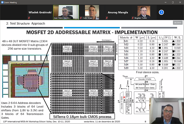
[8] Statistical Analysis of MOSFET extracted parameters for n-MOS mismatch modeling.
Juan Pablo Martinez Brito
CEITEC SA/UFRGS (BR)

[9] Rapid multiscale simulation of nanoscale MOSFETs: Is an interplay between compact models and NEGF possible?
Alexander Kloes
NanoP, THM University of Applied Sciences (D)


[10] The Effect of Non Rectangular MOS Channels in Modelling High Voltage Lateral MOS
Marco Sambi, Lorenzo Labate, Simona Cozzi, Nicola Holzer
STMicroelectronics (I)

MOS-AK session IV
Chair: Daniel Tomaszewski, Lukasiewicz - IMiF, Warsaw (PL)

[11] Nonlinear Embedding Model for the Accelerated Design of PAs with the ASM-HEMT model
Patrick Roblin*, Miles Lindquist*, Nicholas Miller+ and Marek Mierzwinski^
*The Ohio State University, AFRL+, Keysight Corp.^ (USA)

[12] New analytical model for AOSTFTs
Antonio Cerdeira, Yoanlys Hernandez-Barrios, Magali Estrada, Benjamin Iniguez
CINVESTAV (MX) and URV (SP)

[13] Unifying the Modeling of Charge Trapping in RTN, 1/f Noise and BTI
Gilson Wirth
UFRGS (BR)

[14] SPICE Modeling for Display Technologies
Bogdan Tudor
Silvaco (USA)

MOS-AK attendees group photo of 2nd MOS-AK workshop day:

MOS-AK attendees group photo (1)

MOS-AK attendees group photo (2)


Sep 17, 2020

[paper] Compact Model for MoS2 FETs

A physics-based compact model for MoS2 field-effect transistors
considering the band-tail effect and contact resistance
Yuan Liu1, Jiawei Zeng2, Zeqi Zhu1, Xiao Dong2 and WanLing Deng3
Japan Society of Applied Physics; Accepted Manuscript online 11 September 2020
1Guangdong University of Technology, Guangzhou, Guangdong, CHINA
2Jinan University, Guangzhou, Guangdong, CHINA
3Electronic Engineering, Jinan University, Guangzhou, GuangDong, 510630, CHINA

Abstract: In this paper, we present a compact surface-potential-based drain current model in molybdenum disulfide (MoS2) field-effect transistors (FETs). Considering variable range hopping (VRH) transport via band-tail states in MoS2 transistors, an explicit solution for surface potential has been derived and it provides a good description over different regions of operation by comparisons with numerical data. Based on charge-sheet model (CSM) which applies to drift-diffusion transport, the current expression including contact resistance and velocity saturation effect is developed. Furthermore, the presented model is validated and shows a good agreement with experiment data for MoS2 FETs. Keywords: molybdenum disulfide (MoS2), surface potential, current expression.


Jul 24, 2020

[paper] Vectorizing Device Model Evaluation in Ngspice

Vectorizing Device Model Evaluation in Ngspice circuit simulator
Florian Ballenegger, Anamosic Ballenegger Design
Preprint July 2020

Abstract: A method improving the execution speed of electrical circuit simulation using vector processing is proposed. The BSIM3V32 semi-conductor device model for the open-source Ngspice simulator has been re-written for evaluating multiple device instances of the same model at once using Single Instruction Multiple Data (SIMD) processor instructions. While parallel evaluation of device model was already available using multiprocessing, the proposed method can achieve the same speed-up using less processor resources, thus allowing to do more parallel independent simulations for statistical analysis.
In Conclusion: Only the BSIM3V32 device model was modified to use vector processing. Other device models would of course also benefit from the proposed method. In particular interest would be the EKV model https://github.com/ekv26/model, as the calculations in this symmetric model are more linear with fewer conditional branches and could be vectorized more efficently.  The source code of the modified BSIM3V3 model is available at https://www.anamosic.com/pages/ngspice.html

Jun 15, 2020

[paper] Organic Permeable Base Transistors

Darbandy, G., Dollinger, F., Formánek, P., Hübner, R., Resch, S., Roemer, C., Fischer, A., Leo, K., Kloes, A., Kleemann, H., 
Unraveling Structure and Device Operation of Organic Permeable Base Transistors
Adv. Electron. Mater. 2020, 2000230 
DOI 10.1002/aelm.202000230

Abstract: Organic permeable base transistors (OPBTs) are of great interest for flexible electronic circuits, as they offer very large on‐current density and a record‐high transition frequency. They rely on a vertical device architecture with current transport through native pinholes in a central base electrode. This study investigates the impact of pinhole density and pinhole diameter on the DC device performance in OPBTs based on experimental data and TCAD simulation results. A pinhole density of N Pin = 54 µm−2 and pinhole diameters around L Pin = 15 nm are found in the devices. Simulations show that a variation of pinhole diameter and density around these numbers has only a minor impact on the DC device characteristics. A variation of the pinhole diameter and density by up to 100% lead to a deviation of less than 4% in threshold voltage, on/off current ratio, and subthreshold slope. Hence, the fabrication of OPBTs with reliable device characteristics is possible regardless of statistical deviations in thin film formation.
Fig.: Device stack of an OPBT. The central base electrode is permeable to electrons. The device current flows between emitter and collector, while the base layer is passivated by an oxide layer.
The device current can be modulated by the base‐emitter voltage VBE

Acknowledgements: G.D. and F.D. contributed equally to this work. This project was funded by the German Research Foundation (DFG) under the grants KL 1042/9‐2 and LE 747/52‐2 (SPP FFlexCom) and by the European Community’s Seventh Framework Programme under Grant Agreement No. FP7‐267995 (NUDEV). This work was supported in part by the German Research Foundation (DFG) within the Cluster of Excellence Center for Advancing Electronics Dresden (cfaed) and the DFG project HEFOS (Grant No. FI 2449/1‐1). Furthermore, the use of HZDR Ion Beam Center TEM facilities and the funding of TEM Talos by the German Federal Ministry of Education of Research (BMBF; grant No. 03SF0451) in the frame‐work of HEMCP are acknowledged. The authors thank Tobias Günther and Andreas Wendel of IAPP for sample preparation.

May 11, 2020

[paper] BSIM-HV: High-Voltage MOSFET Model

H. Agarwal , Member, IEEE, C. Gupta , Graduate Student Member, IEEE, R. Goel , Graduate Student Member, IEEE, P. Kushwaha , Member, IEEE, Y.-K. Lin , Graduate Student Member, IEEE, M.-Y. Kao , Graduate Student Member, IEEE, J.-P. Duarte , Graduate Student Member, IEEE, H.-L. Chang , Member, IEEE, Y. S. Chauhan , Senior Member, IEEE, S. Salahuddin, Fellow, IEEE, and C. Hu, Life Fellow, IEEE
BSIM-HV: High-Voltage MOSFET Model Including Quasi-Saturation and Self-Heating Effect
IEEE TED, vol. 66, no. 10, pp. 4258-4263, Oct. 2019
doi: 10.1109/TED.2019.2933611

Abstract - A BSIM-based compact model for a high-voltage MOSFET is presented. The model uses the BSIM-BULK (formerly BSIM6) model at its core, which has been extended to include the overlap capacitance due to the drift region as well as quasi-saturation effect. The model is symmetric and continuous, is validated with the TCAD simulations and experimental 35- and 90V LDMOS and 40V VDMOS transistors, and shows excellent agreement.
FIG: Schematic of the LDMOS. Lightly doped n-region constitutes the drain. Majority of the applied drain voltage drops across this region, which protects the intrinsic transistor region from breakdown.
Manuscript received March 3, 2019; revised May 23, 2019 and July 24, 2019; accepted July 31, 2019. Date of publication August 26, 2019; date of current version September 20, 2019. This work was supported in part by the members of the Berkeley Center for Negative Capacitance Technology and the members of the Berkeley Device Modeling Center. The review of this article was arranged by Editor B. Iñiguez.

[paper] Compact Device Models for FinFET and Beyond

D. D. Lu, M. V. Dunga, A. M. Niknejad, C.Bing Hu, F.-X. Liang, W.-C. Hung, J. Lee, C.-H. Hsu
and M.-H. Chiang,
Compact device models for FinFET and beyond
ArXiv, vol. abs/2005.02580, 2020

Abstract - Compact device models play a significant role in connecting device technology and circuit design. BSIM-CMG and BSIM-IMG are industry standard compact models suited for the FinFET and UTBB technologies, respectively. Its surface potential based modeling framework and symmetry preserving properties make them suitable for both analog/RF and digital design. In the era of artificial intelligence / deep learning, compact models further enhanced our ability to explore RRAM and other NVM-based neuromorphic circuits. We have demonstrated simulation of RRAM neuromorphic circuits with Verilog-A based compact model at NCKU. Further abstraction with macromodels is performed to enable larger scale machine learning simulation.
Fig: Simulation of a novel floating - gate synaptic transistor. (a) Device structure with separate negative feedback gate (nfb) for programming and synaptic gate (sg) readout. (b) Equivalent circuit diagram for compact modeling 
Acknowledgements - The authors would like to express sincere gratitude to Chip Implementation Center (CIC), Hsinchu, Taiwan for providing SPICE simulation environment for RRAM simulations.

Apr 1, 2020

[C4P] ESSDERC TRACK3 Compact Modeling


European ESSDERC/ESSCIRC conference will be organized in Grenoble (F) on Sept.14-18, 2020 with its integral TRACK3: Compact Modeling and Process/Device Simulation which is open for submissions, now. You and all your R&D partners are welcome to submit a modeling paper. The paper submission deadline is April 17, 2020

TRACK3: Compact modeling and process/device simulation (including TCAD and advanced simulation techniques and studies)  focuses on following domains among other R&D topics:
  • Compact/SPICE modeling of electronic, optical, organic, and hybrid devices and their IC implementation and interconnection. 
  • Verilog-A models of the semiconductor devices (including Bio/Med sensors, MEMS, Microwave, RF, HV and Power, emerging technologies and novel devices)
  • Compact/SPICE parameter extraction
  • Performance evaluation and open source (FOSS) benchmarking/implementation methodologies
  • Modeling of interactions between process, device and circuit design, 
  • Foundry/Fabless interface strategies
  • Numerical TCAD, analytical, statistical modeling and simulation of electronic, optical and hybrid devices, interconnect, isolation and 2D/3D integration
  • Aspects of materials, fabrication processes and devices e.g. advanced physical phenomena (quantum mechanical and non-stationary transport phenomena, ballistic transport, ...)
  • Optical, mechanical or electro-thermal modeling and simulation
  • DfM, ageing, reliability of materials and devices
Please share our TRACK3 C4P with all your academic and industrial R&D partners active in the compact/SPICE modeling, Verilog-A standardization and TCAD/EDA simulations. Of course, your and your research team proactive contribution to our TRACK3 is more than welcome. I do hope that despite of a last minute notice, with your help, we will be able to draw even more attention to the ESSDERC/ESSCIRC Conference and, in particular, our modeling TRACK3


Jan 23, 2020

9th SiNANO Modeling and Simulation Summer School

2020 Summer School on advanced modeling and simulation of conventional and novel nano-CMOS devices, to be held in Glasgow, Scotland with technical sessions from the 29th June – 3rd July 2020


This year the SINANO Summer School will target multi-scale modeling and simulation of semiconductor devices. It includes a total of 15 lectures targeting topics related to the modelling and simulation as well as fabrication and characterization of different types of semiconductor nanoelectronic devices. The Summer School will cover to the following topics:
  • Novel nanoelectronics devices and corresponding modelling challenges.
  • Material modeling and atomic scale device simulation.
  • Quantum transport and simulations.
  • Monte Carlo and Wigner Monte Carlo simulations.
  • Compact modeling
  • Process simulations
  • Design Technology Co-Optimization (DTCO)

Confirmed invited speakers:
Speaker
Organisation
Speaker
Organisation
Dr. Victor Moroz
Synopsys
Prof. Gerhard Klimeck
Purdue University
Prof. Adrian Ionescu
EPFL
Prof. Philippe Dollfus
University Paris Sud
Prof. Mathieu Luisier 
ETH
Prof. Nicola Marzari
EPFL
Dr. Kirsten Moselund
IBM Zurich
Prof. Francisco Gamiz
University of Granada
Dr. Kurt Stokbro
Synopsys
Prof. Max Fischetti
The Uni. Texas - Dallas
Prof. Jurgen Lorenz
IISB Fraunhofer
Prof. Tibor Grasser
TU Vienna
Dr. Yann-Michel Niquet
CEA Leti
Dr. Cory Weber
Intel USA
Dr. Plamen Asenov
Synopsys


For more information please see the flyer and this website: https://www.gla.ac.uk/events/conferences/sinano2020/

Jan 20, 2020

Qucs-S as R&D design software

Qucs-S 

is not a simple circuit simulator, but also a research software. Please cite your R&D articles, if you are using Qucs-S in your research.

Documentation

Publications

Qucs-S is not a simple circuit simulator, but also a research software. Please cite our articles, if you are using Qucs-S in your research.
  1. Brinson, M. E., and Kuznetsov, V. (2016) A new approach to compact semiconductor device modelling with Qucs Verilog-A analogue module synthesis. Int. J. Numer. Model., 29: 1070-1088. (BibTeX)
  2. D. Tomaszewski, G. Głuszko, M. Brinson, V. Kuznetsov and W. Grabinski, "FOSS as an efficient tool for extraction of MOSFET compact model parameters," 2016 MIXDES - 23rd International Conference Mixed Design of Integrated Circuits and Systems, Lodz, 2016, pp. 68-73. (BibTeX)
  3. M. Brinson and V. Kuznetsov, "Qucs-0.0.19S: A new open-source circuit simulator and its application for hardware design," 2016 International Siberian Conference on Control and Communications (SIBCON), Moscow, 2016, pp. 1-5. (BibTeX)
  4. M. Brinson and V. Kuznetsov, "Improvements in Qucs-S equation-defined modelling of semiconductor devices and IC's," 2017 MIXDES - 24th International Conference "Mixed Design of Integrated Circuits and Systems, Bydgoszcz, 2017, pp. 137-142. (BibTeX)
  5. M. Brinson and V. Kuznetsov, "Extended behavioural device modelling and circuit simulation with Qucs-S" International Journal of Electronics, 2017, pp.1 - 14 (BibTeX)

Jan 3, 2020

C4P Special Issue JEDS on Compact Modeling

Call for papers for a Special Issue
of IEEE Journal of the Electron Devices Society
on “Compact Modeling of Semiconductor Devices”
Submission deadline: April 1, 2020 MAY 15, 2020

In order to exploit the full potential of semiconductor devices in circuit design, compact device models are critically needed. Compact device models are the vehicle that allow the design of circuits using the targeted devices. Predictive and physically-based compact device models are required to accelerate development cycles and tackle issues of device efficiency, manufacturing yield and product stability. The performance/accuracy of the design software is dependent on the availability of accurate compact device models. 
Compact models should accurately capture the physics of the device in all operation regimes, but at the same time they should also have an analytical or semi-analytical formulation to be used in automated design tools for the simulation of circuits containing several or many devices. Furthermore, compact models can also be used as a tool to make realistic estimations of the performances of future devices following technological trends.
The lack of adequate compact models for a number of emerging devices is mostly due to the insufficient understanding of the physical phenomena which determine their behaviors. Regarding many emerging non-silicon devices, circuit and system designers very often rely on empirical behavioral macro-models and/or use existing silicon device compact models based on the conventional understanding of transport processes. However, for these emerging non-silicon devices, neither approach provides a fully adequate device description under all operation conditions, and therefore does not allow accurate production quality design.

Suggested topics include but not limited to:

1. Silicon MOSFET modeling
a. Advanced Bulk MOSFETs
b. SOI MOSFETs
c. Multi-Gate MOSFETs: Double-Gate MOSFETs, Surrounding-Gate MOSFETs, FinFETs, nanosheet MOSFETs, UTB SOI MOSFETs, etc.
d. Junctionless MuGFETs
e. Power and high voltage MOSFETs
2. Junction-based and compound semiconductor FET modeling:
a. Advanced MESFETs
b. Advanced HEMTs
c. III-V and III-N MOSFETs
d. Advanced JFETs
3. Diode and bipolar transistor modeling:
a. Advanced BJTs
b. HBTs
c. IGBTs
d. pn and pin diodes
e. Varactors
4. Emerging transistor modeling:
a. Tunnel FETs
b. Molecular transistors
c. Single Electron Transistors
d. Quantum Dot Transistors
e. Negative Capacitance Transistors
5. Emerging semiconductor devices
Memories, MRAM, PCRAM, etc.
Memristors
Spintronic devices
Layered/2D semiconductor devices
Graphene-based devices
6. TFT
a. a-Si:H TFTs
b. Polycrystalline Si TFTs
c. OTFTs and OECTs
d. Oxide TFTs
e. Single-crystal TFts
7. Modeling of physical effects
a. Noise
b. High frequency operation
c. Cryogenic conditions
d. Mismatch
e. Strain
f. High energy particle interactions in ICs (Cosmic rays and energy beams)
g. ESD events
h. Ballistic and quasi-ballistic transport
i. Layout dependent effects
8. Photonic devices
a. LEDs and OLEDs
b. Photodiodes
c. Solar cells
d. Photodetectors
e. SPADs
f. Photonic Crystals
9. Parameter extraction methods
a. Direct extraction methods
b. Global optimization methods

Submission instructions: Manuscripts should be submitted in a double column format using an IEEE style file. Please, visit https://ieeeauthorcenter.iece.org/create-your-ieee- article/use-authoring-toolsand-ieee-article-templates/ieee-article-templates/templates-for- transactions/ to download the templates. When submitting your manuscript through the IEEE’s web-based ScholarOne Author Submission and Peer Review System (https://mc.manuscriptcentral.com/jeds), please indicate that your submission is for this special issue.

Guest Editor in Chief:
  • Benjamin Iniguez, Universitat Rovira i Virgili, Tarragona, Spain
Guest Associate Editors:
  • Yogesh Chauhan, IIT Kanpur (IN) 
  • Slobodan Mijalkovic, Silvaco Europe Ltd., St.Ives (UK) 
  • Kejfun Xia, NXP Semiconductors, Phoenix, AZ (USA) 
  • Jhung-Suk Goo, Global Foundries, Sunnyvale, CA (USA), 
  • Marcelo Pavanello, Centro Universitario da FEI, Sao Paulo (BR), 
  • Marek Mierzwinski, Keysight Technologies, Santa Rosa, CA (USA)
  • Wladek Grabinski, GMC Consulting, Commugny (CH)
Please, direct all communications to Marlene James at m.james@ieee.org

DOI 10.1109/TED.2019.2960953

Nov 29, 2019

PhD Positions at Institute for Microelectronics/TU Wien

PhD Positions
on Characterization, Modeling and Circuit Simulation in Microelectronics
Institute for Microelectronics/TU Wien


The Institute for Microelectronics is a world leading research institute focused on the reliability of circuit components (especially transistors). In addition to conventional Si transistors, the behavior of SiC devices designed for high-power applications is also at the center of interest. The broad field of research conducted at the Institute of Microelectronics ranges from characterization, physical modeling and ab-initio simulations to compact modeling and circuit simulation. For the characterization of transistors, the Institute for Microelectronics has a modern laboratory equipped with commercial and custom-built measurement instruments. To explain the experimental data, elaborate physical models are developed and constantly improved. The models are directly incorporated into state-of-the-art device simulators, i.e. MinimosNT and Comphy. To perform computationally expensive simulations a modern computer cluster is while for circuit simulations Cadence and Synopsis spice simulators are available.

The institute is currently looking for highly talented and motivated young researchers to join the team in one of the following areas:
  • Physical modeling of silicon-carbide transistors
  • Single-defect characterization of low-noise silicon transistors
  • Development of custom-made measurement instruments
  • Circuit simulations using advanced implementation of reliability models in Verilog-A for SPICE
For the positions knowledge in one or more of the following areas is advantageous to complement our team:
  • C/C++ and Python
  • Semiconductor device physics
  • Circuit simulation
  • Implementation of new compact/physical models
  • Handling of device/circuit simulators
  • Design of discrete analog circuits and hardware/software solutions
  • Wafer probers and instruments for microelectronics
  • Keithley instruments and scripting language LUA
  • Measurement techniques in microelectronics (MSM, C(V), DLTS, charge pumping etc.)
As a teaching institution, knowledge transfer and close cooperation with students are very importance. The applicants should like to work together with students and supervise Master’s and Bachelor theses.

Starting Date: As soon as possible

Salary: Three-year positions (40hours/week) are in accordance with the salary regulations of the Austrian Science Fund. The gross annual salary is approximately EUR 40,300

Application Material: Please provide a detailed CV, your collective certificates, your Master’s thesis (weblink or PDF), and a single-page motivation letter (discussing relevant previous experience related to the desired skills and experiences) and summarize your motives for joining us.

Application: Please submit your application to jobs@iue.tuwien.ac.at.
Application Deadline: The positions will remain open until filled.

Nov 19, 2019

MOS-AK India #45395 is now published in IEEE Xplore

2019 IEEE Conference on Modeling of Systems Circuits and Devices 
(MOS-AK India) - #45395 
is now published in IEEE Xplore

Conference Record #45395

Dear Arifuddin Sohel, Desai UB, Govindacharyulu P.A, Wladek Grabinski, Venkatesh N

Congratulations! 2019 IEEE Conference on Modeling of Systems Circuits and Devices (MOS-AK India) has been posted to the IEEE Xplore digital library effective 2019-11-18.

Along with publication in IEEE Xplore, IEEE assures wide distribution of conference proceedings by providing abstracting and indexing information of all individual conference papers to worldwide databases. IEEE makes every reasonable attempt to ensure that abstracts and index entries of content accepted into the program are included in databases provided by independent abstracting and indexing services. Each abstracting and indexing partner makes its own editorial decision on what content to include. IEEE cannot guarantee entries are included in any particular database.

IEEE Meetings, Conferences & Events (MCE)
445 Hoes Lane, Piscataway, NJ 08854 USA
IEEE: Advancing Technology for Humanity

Oct 10, 2019

article with 700 reads

Wladek Grabinski, Matt Bucher,Jean-Michel Sallese and François Krummenacher
Journal of Telecommunications and Information Technology (3-4):31-42, March 2000


Oct 3, 2019

[IEEE EDS Update] MIXDES 2019, Rzeszów (PL)

26th International Conference “Mixed Design of Integrated Circuits and Systems"'
MIXDES 2019 
By Marcin Janicki

On June 27–29, 2019, Rzeszów, Poland, the International Conference MIXDES 2019 took place. The event was organized by the Lodz University of Technology together with the Warsaw University of Technology. The conference was co-sponsored by Poland Section IEEE ED & CAS Societies, Polish Academy of Sciences (Section of Microelectronics and Electron Technology), and Commission of Electronics and Photonics of Polish National Committee of International Union of Radio Science—URSI. The 3-day conference program included 97 presentations from 28 countries. The following six general invited talks were presented during the conference plenary sessions:
  • Advanced MOS Device Technology for Low Power Logic LSI Shinichi Takagi (The University of Tokyo, Japan)
  • Quantum Bits and Quantum Computing Architecture Farzan Jazaeri (EPFL, Switzerland)
  • Towards Energy-Autonomous Integrated Systems Through Ultra-low Voltage Analog IC Design Viera Stopjaková (Slovak University of Technology in Bratislava, Slovakia)
  • THz Technologies and Applications Thomas Skotnicki (Institute of High Pressure Physics PAS, Poland)
  • What is Killing Moore’s Law? Challenges in Advanced FinFET Technology Integration Arkadiusz Malinowski (GLOBALFOUNDRIES, USA)
  • Yield and Reliability Challenges at 7nm and Below Andrzej Strojwąs (Carnegie Mellon University, USA)
The sessions also included presentations in the frame of four special sessions:
  • Compact Modeling for Nanoelectronics organized by D. Tomaszewski (Institute of Electron Technology, Poland) and W. Grabiński (GMC, Switzerland)
  • Intelligent Distributed Systems organized by M. Drozd (LTC Sp. z o.o., Poland), R. Sztoch, P. Sztoch (FINN Sp. z o.o., Poland), B. Sakowicz and D. Makowski (Lodz University of Technology, Poland)
  • Large Scale Research Facilities organized by A. Napieralski, W. Cichalewski (Lodz University of Technology, Poland)
  • Thermonuclear Fusion Projects organized by S. Simrock (ITER, France), D. Makowski (Lodz University of Technology, Poland), D. Bocian and M. Scholz (Institute of Nuclear Physics, Poland
The next MIXDES 2020 Conference will take place in Wrocław, Poland. The Preliminary Call for Papers is available at http://www.mixdes.org/downloads/call2020.pdf. More information about the past and next MIXDES Conferences can be found at http://www.mixdes.org.
Edited by Mariusz Orlikowski
MIXDES 2019 Conference Secretary

Aug 12, 2019

[papers] Compact Modeling

Q. C. Nguyen, P. Tounsi, J. Fradin and J. Reynes, "Development of SiC MOSFET Electrical Model and Experimental Validation: Improvement and Reduction of Parameter Number," 2019 MIXDES - 26th International Conference "Mixed Design of Integrated Circuits and Systems", Rzeszów, Poland, 2019, pp. 298-301.
doi: 10.23919/MIXDES.2019.8787050
Abstract: In this work, a new approach for electrical modeling of Silicon Carbide (SiC) MOSFET is presented. The developed model is inspired from the Curtice model which is using a mathematic function reflecting MOSFET output characteristics. The first simulation results showed good agreement with measurements. Improvement is needed in order to increase model accuracy and to take into account the influence of the junction temperature on device characteristics.

D. Kasprowicz, "Semiconductor Device Parameter Extraction Based on I–V Measurements and Simulation," 2019 MIXDES - 26th International Conference "Mixed Design of Integrated Circuits and Systems", Rzeszów, Poland, 2019, pp. 321-326.
doi: 10.23919/MIXDES.2019.8787195
Abstract: The paper presents a method for extracting the physical parameters of a semiconductor device based on the measurements of its electrical response (e.g. transfer characteristics) combined with simulation. Such extraction is usually performed by an optimization algorithm seeking device-parameter values that minimize the difference between the measured response and its simulated equivalent. The proposed approach needs only an average of 13 objective-function evaluations, i.e. device simulations, to extract three parameters of a single device. If the parameters of a group of devices of the same type are to be extracted, the average number of simulations drops to four per device. This number is much smaller than in conventional optimization procedures. Thus, the proposed procedure can be used even in the absence of an accurate compact model, when time-consuming TCAD simulation must be used to determine the device’s response.

D. Tomaszewski, J. Malesińska, G. Głuszko and K. Kucharski, "Current vs Substrate Bias Characteristics of MOSFETs as a Tool for Parameter Extraction," 2019 MIXDES - 26th International Conference "Mixed Design of Integrated Circuits and Systems", Rzeszów, Poland, 2019, pp. 87-91.
doi: 10.23919/MIXDES.2019.8787068
Abstract: An application of the drain current vs substrate bias characteristics of MOSFETs for the device parameter extraction is presented. Modeling of the substrate bias effect on the MOSFET drain current is briefly discussed. A method of the MOSFET characterization is formulated. It requires a measurement of two I(V) characteristics, including the ID(VBS) smooth curve measured in a "sweep" mode. The method allows to extract the threshold voltage parameters and to estimate the in-depth doping profile in the substrate. The proposed approach is demonstrated using I(V) data of the MOSFETs manufactured in ITE in a bulk CMOS process.