Recent, 16th International MOS-AK Workshop hosted by Keysight Technologies in Santa Clara, CA 95051, on Dec. 13, 2023, featured invited talks from EDS Distinguished Lecturers (DL) and leading experts in the field. The selected R&D topics include self-heating and trapping effects in GaN HEMTs, Si2 CMC updates, integrated antennas, European open source PDK Initiative, re-energizing analog design using the open-source ecosystem, SPICE modeling of Si, GaN and SiC power FET devices, new models to capture generic device physics, quantum computing and simulation, open source neuromorphic computing, and custom IC designs using open source OpenFASOC. The workshop presentations are listed below:
| T_0 | Opening and MOS-AK Intro Wladek Grabinski MOS-AK (EU) |
| T_1 | Welcome and A Brief History of Keysight Nilesh Kamdar Keysight EDA |
| T_2 | Accurate Modeling of the Self-Heating and Trapping Effects in GaN HEMTs DOI:10.5281/zenodo.1042343 Yiao Li Keysight Technologies |
| T_3 | Si2 Compact Model Coalition 2023 Updates DOI: 10.5281/zenodo.10423502 Peter M. Lee and Colin Shaw Si2 Compact Model Coalition |
| T_4 | Some efforts toward the modeling of integrated antennas DOI: 10.5281/zenodo.10401753 Roberto S. Murphy-Arteaga, IEEE EDS DL INAOE, Puebla, Mexico |
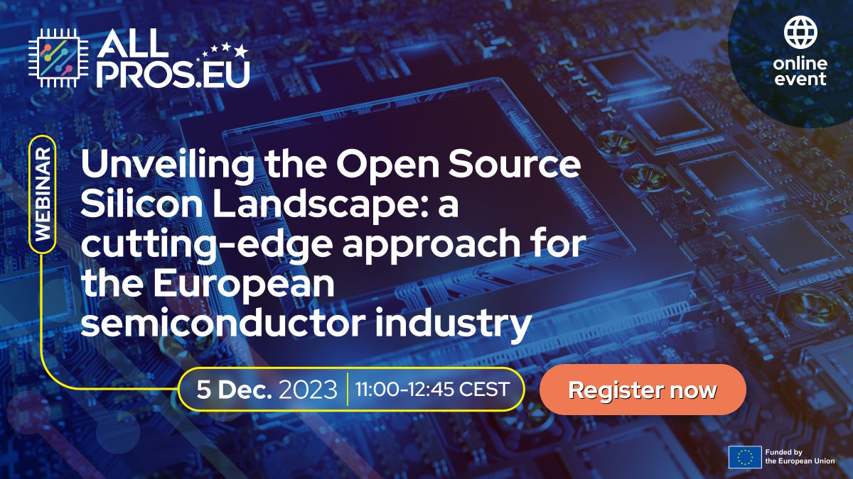
| T_5 | European Open Source PDK Initiative DOI: 10.5281/zenodo.10423518 Wladek Grabinski, IEEE EDS DL MOS-AK (EU) |
| T_6 | Re-Energizing Analog Design using the Open-Source Ecosystem DOI: 10.5281/zenodo.10423729 Boris Murmann University of Hawaii |
| T_7 | SPICE Modeling of Si, GaN and SiC Power FET Devices DOI: 10.5281/zenodo.10423740 Bogdan Tudor Silvaco, Inc. |
| T_8 | A Transformer-Based Foundation Model to Capture Generic Device Physics DOI: 10.5281/zenodo.10423765 Hyunbo Cho Alsemy Inc. |
| T_9 | Quantum Computing and Simulation DOI: 10.5281/zenodo.10423785 Hiu Yung Wong San Jose State University |
| T_10 | Open Source Neuromorphic Computing DOI: 10.5281/zenodo.10423809 Jason Eshraghian // online Neuromorphic Computing Group at UC Santa Cruz |
| T_11 | Accelerating custom Circuits using OpenFASOC DOI: 10.5281/zenodo.xxx Mehdi Saligane // online UMich (US) |
The MOS-AK Association plans to continue its standardization efforts by organizing future compact modeling meetings, workshops and panels around the globe thru the 2024 Year, including:
- FOSDEM, Bruxelles (BE) Feb. 3-4, 2024
- MOS-AK/EDTM, Bangalore (IN) March 3-6, 2024
- 6th MOS-AK/LADEC, Guatemala City (GT) May 8-10, 2024
- Special CM Session, MIXDES, Gdańsk (PL) June 27-29, 2024
- 8th Sino MOS-AK Workshop (CN), August 2024
- 21st MOS-AK at ESSERC, Bruges (BE) Sept. 9-12, 2024
- 17th MOS-AK/Silicon Valley, (CMC/IEDM Timeframe) Dec. 2024
-- W.Grabinski on the behalf of the International MOS-AK Committee
22122023
You received this message because you are subscribed to the Google Groups "mos-ak" group.
To unsubscribe from this group and stop receiving emails from it, send an email to mos-ak+unsubscribe@googlegroups.com.
To view this discussion on the web visit https://groups.google.com/d/msgid/mos-ak/CALp-Rj8Q4tx_m0v9PRfzkvsOMZdzhdj1YQr4Be-OT%2BcWBOYPnA%40mail.gmail.com.