Showing posts with label FET. Show all posts

Oct 6, 2023

[book chapters] Equation-Based Compact Modeling


Debnath, P., Sarkar, B., & Chanda, M. (Eds.). (2023).
Differential Equation Based Solutions 
for Emerging Real-Time Problems
(1st ed.). CRC Press 
DOI 10.1201/9781003227847


Chapter: Differential Equation-Based Compact 2-D Modeling of Asymmetric Gate Oxide Heterojunction Tunnel FET; By: Sudipta Ghosh, Arghyadeep Sarkar

Abstract: Tunnel Field Effect Transistor (TFET) has emerged as an effective alternative device to replace MOSFET for a few decades. The major drawbacks of MOSFET devices are the short-channel effects, due to which the leakage current increases with a decrease in device dimension. So, scaling down TFET is more efficacious than that of MOSFETs. Sub-threshold swing (SS) is another advantageous characteristic of TFET devices for high-speed digital applications. In TFETs the SS could be well below 60 mV/decade, which is the thermal limit for MOSFET devices and therefore makes it more suitable than MOSFET for faster switching applications. It is observed from the literature studies that the performances of the TFET devices have been explored thoroughly by using 2-D TCAD simulation but an analytical model is always essential to understand the physical behavior of the device and the physics behind this; which facilitates further, the analysis of the device performances at circuit level as and when implemented.

Chapter: Differential Equation-Based Analytical Modeling of the Characteristics Parameters of the Junctionless MOSFET-Based Label-Free Biosensors; by: Manash Chanda, Papiya Debnath, Avtar Singh

Abstract: Recently Field Effect transistor (FET)-based biosensing applications have gained significant attention due to the demand for quick and accurate diagnosis of different enzymes, proteins, DNA, viruses, etc; cost-effective fabrication process; portability and better sensitivity and selectivity compared to the existing biosensors. FET is basically a three-terminal device with source, drain, and gate terminals. Basically, the gate terminal controls the current flow between the source and drain terminals. In FETs, first, a nanogap is created in the oxide layer or in the gate by etching adequate materials. When the biomolecules are trapped inside the nanocavity then the surface potentials change and also the threshold voltage varies. As a result, the output current also changes. Finally, by measuring the changes in the threshold voltage or the device current, one can easily detect the biomolecules easily.

Jul 31, 2023

[book] Negative Capacitance Field Effect Transistors


Negative Capacitance Field Effect Transistors
Physics, Design, Modeling and Applications


Edited By Young Suh Song, Shubham Tayal, Shiromani Balmukund Rahi, Abhishek Kumar Upadhyay


Pages 63 Color & 7 B/W Illustrations
ISBN 9781032445311 176 Sept. 29, 2023 by CRC Press


Description
This book aims to provide information in the ever-growing field of low-power electronic devices and their applications in portable device, wireless communication, sensor, and circuit domains. Negative Capacitance Field Effect Transistor: Physics, Design, Modeling and Applications, discusses low-power semiconductor technology and addresses state-of-art techniques such as negative-capacitance field-effect transistors and tunnel field-effect transistors. The book is broken up into four parts. Part one discusses foundations of low-power electronics including the challenges and demands and concepts like subthreshold swing. Part two discusses the basic operations of negative-capacitance field-effect transistor (NC-FET) and Tunnel Field-effect Transistor (TFET). Part three covers industrial applications including cryogenics and biosensors with NC-FET. This book is designed to be one-stop guidebook for students and academic researchers, to understand recent trends in the IT industry and semiconductor industry. It will also be of interest to researchers in the field of nanodevices like NC-FET, FinFET, Tunnel FET, and device-circuit codesign.

Table of Contents
Chapter 1 Recent Challenges in IT and Semiconductor Industry: From Von Neumann Architecture to the Future
Young Suh Song, Shiromani Balmukund Rahi, Navjeet Bagga, Sunil Rathore, Rajeewa Kumar Jaisawal, P. Vimala, Neha Paras, K. Srinivasa Rao
Chapter 2 Technical Demands of Low-Power Electronics
Soha Maqbool Bhat, Pooran Singh, Ramakant Yadav, Shiromani Balmukund Rahi, Billel Smaani, Abhishek Kumar Upadhyay, Young Suh Song
Chapter 3 Negative capacitance Field Effect Transistors: Concept and Technology
Ball Mukund Mani Tripathi
Chapter 4 Basic Operation Principle of Negative Capacitance Field Effect Transistor
Malvika, Bijit Choudhuri, Kavicharan Mummaneni
Chapter 5 Basic Operational Principle of Anti-ferroelectric Materials and Ferroelectric Materials
Umesh Chandra Bind, Shiromani Balmukund Rahi
Chapter 6 Basic Operation Principle of Optimized NCFET: Amplification Perspective
S. Yadav, P.N Kondekar, B. Awadhiya
Chapter 7 Spin Based Magnetic Devices With Spintronics
Asif Rasool, Shahnaz kossar, R.Amiruddin
Chapter 8 Mathematical Approach for Future Semiconductor Roadmap
Shiromani Balmukund Rahi,Abhishek Kumar Upadhyay, Young Suh Song, Nidhi Sahni, Ramakant Yadav, Umesh Chandra Bind,Guenifi Naima,Billel Smaani,Chandan Kumar Pandey,Samir Labiod, T.S. Arun Samul,Hanumanl Lal, H. Bijo Josheph
Chapter 9 Mathematical Approach for Foundation of Negative Capacitance Technology
Shiromani Balmukund Rahi,Abhishek Kumar Upadhyay, Young Suh Song, Nidhi Sahni, Ramakant Yadav, Umesh Chandra Bind,Guenifi Naima,Billel Smaani,Chandan Kumar Pandey,Samir Labiod, T.S. Arun Samul,Hanumanl Lal, H. Bijo Josheph


Jul 20, 2023

[paper] THz FET Modeling

Adam Gleichman1, Kindred Griffis1, and Sergey V. Baryshev1,2
Useful Circuit Analogies to Model THz Field Effect Transistors
arXiv:2307.07488v1 [physics.app-ph] 14 Jul 2023

1) Department of Electrical and Computer Engineering, Michigan State University, USA
2) Department of Chemical Engineering and Materials Science, Michigan State University, USA

Anstract: The electron fluid model in plasmonic field effect transistor (FET) operation is related to the behavior of a radio-frequency (RF) cavity. This new understanding led to finding the relationships between physical device parameters and equivalent circuit components in traditional parallel resistor, inductor, and capacitor (RLC) and transmission models for cavity structures. Verification of these models is performed using PSpice to simulate the frequency dependent.
FIG: RLC Lumped THz FET Model


Jul 12, 2023

[chapter] GAA Transistors

Srivastava, Shobhit, and Abhishek Acharya
Challenges and future scope of gate-all-around (GAA) transistors
in "Device Circuit Co-Design Issues in FETs"; 
Shubham Tayal et al. (Editors)
231 CRC Press, 22 Aug 2023 - Technology & Engineering

Introduction: No doubt, FinFET technology is the slogger of today's semiconductor world. But as demand for further scaling with a desire for ultra-low-power and high-speed applications results in undesired short-channel effects, a new transistor is required. This is where gate-all-around (GAA) devices come into being. The GAA structure helps to mitigate unwanted short-channel effects by enhancing channel controllability. In GAAFETS, the channel surrounds all of its sides through a high-K and interfacial oxide layer. Thanks to science and technological innovation, the GAAFET family brings together different transistors and their competitive benefits. This chapter tries to answer why and how 3D devices emerge. In addition to the limitation of FinFET (a 3D device, gate surrounded by three sides), it further talks about the scope and challenges of different competitive GAAFET members (nanowire FET, nanosheet FET, junctionless nanosheet FET, complementary PET, and forksheet FET) of the GAAFET family. It is worth mentioning that a smaller benefit of the device performance exerts a massive performance enhancement on circuit-level applications. However, the advantages of device enhancement concurrently exaggerate the limitation of devices at circuit-level applications. So, an elaborated idea of GAAFETs holding the benefits and challenges at the circuit is also discussed here.


FIG: Structural evolution of transistors from planar to 3D forksheet FET technology


Jun 14, 2023

[paper] Vertical Junction-Less Nanowire FETs

C. Maneux (University of Bordeaux), C. Mukherjee (CNRS), M. Deng (University of Bordeaux), G. Larrieu (CNRS), Y. WANG, B. Wesling, and H. Rezgui (University of Bordeaux)
Strategies for Characterization and Parameter Extraction of Vertical Junction-Less Nanowire FETs Dedicated to Design Technology Co-Optimization
H02-1863 (Invited) at 243rd ECS Meeting and SOFC-XVIII 
Boston, MA, May 29 - June 2, 2023

Abstract: In the era of emerging computing paradigms and artificial neural networks, hardware and functionality requirements are in the surge. In order to meet low power and latency criteria, new architectures for in-memory computing are being explored as alternatives to traditional von Neumann machines, which requires technological breakthrough at the semiconductor device level such as vertical gate-all-around junctionless nanowire field effect transistors (VNWFET), that can address many process challenges such as downscaling, short-channel effects, compactness and electrostatic control. Its integration in the mainstream design flow is not straightforward and requires design technology co-optimization (DTCO) at an early stage. This invited paper explores strategies for accurate characterization and parameter extraction of the VNWFETs to feed the DTCO compact models

Fig: Final verification using full 3D multiphysics device thermal simulation, accounting for both ballistic and diffusive heat flux

Dec 8, 2021

[paper] Analytical Compact Model Of Cylindrical Junctionless Nanowire FETs

Adelcio M. de Souza, Daniel R. Celino, Regiane Ragi, Murilo A. Romero
Fully analytical compact model for the Q–V and C–V characteristics 
of cylindrical junctionless nanowire FETs
Microelectronics Journal (2021): 105324
DOI: 10.1016/j.mejo.2021.105324
   
University of Sao Paulo (EESC/USP), Sao Carlos (BR)

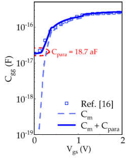
Abstract: This paper develops a new compact model for the Q–V and C–V characteristics of cylindrical junctionless nanowire FETs in which the nanowire radius is large enough, in such a way that quantum confinement effects can be neglected. Our model is fully analytical and valid for all bias regimes, i.e., subthreshold, partial depletion, and accumulation. The obtained Q-V and C–V characteristics, as well as their derivatives, are continuous across the full range of bias voltages. The model is fully physics-based, with no fitting parameters, and it is very intuitive, since it relies on the understanding of the device as a gated resistor. Model validation is performed against previous results in the literature, demonstrating very good agreement.
Fig.  Validation of our C–V model (solid lines) in comparison to numerical results, highlighting the effect of parasitic capacitance. The free-carrier capacitance component from new model is shown in dashed lines. Simulation parameters: tox = 4.5nm, Nd = 1.6E18 cm−3, L = 200nm, VFB = 1.09V and Vds = 0.05V.

Acknowledgments: The authors would like to thank the Brazilian funding agencies CAPES, CNPq, and Fapesp for their financial support: Conselho Nacional de Desenvolvimento Científico e Tecnologico. Grant Number: 303708/2017-4; Coordenaçao de Aperfeiçoamento de Pessoal de Nível Superior; Fundaçao de Amparo a Pesquisa do Estado de Sao Paulo. Grant Number: 18/13537-6.

Nov 16, 2021

[paper] Extended gate FET pH Sensor

Shaiful Bakhtiar Hashim, Zurita Zulkifli, Sukreen Hana Herman
Design and Simulation of Electrochemical Equivalent Circuit for Extended gate FET pH Sensor Based on Experimental Value Using LTSPICE XVII
researchsquare.com: November 11th, 2021
DOI:10.21203/rs.3.rs-1031896/v1
  
College of Engineering, UiTM, Selangor (MY)


Abstract: A SPICE model for extended-gate field-effect transistor (EGFET) based pH sensor was developed using standard discrete components. Capacitors and resistors were used to represent the sensing and reference electrodes in the EGFET sensor system and the values of the discrete component were varied to see the output of the transistor. These variations were done to emulate the EGFET sensor output in different pH values. It was found that the experimental transfer and output characteristics of the EGFET were very similar to those from the SPICE simulation. Other than that, the changes of value components in the equivalent circuit did not affect the transfer and output characteristics graph, but the capacitor value produced significant output variation in the simulation. This can be related to the modification on the equivalent circuit was done with additional voltage, VSB (source to bulk) to produce the different VT values at different pH.
Fig: EGFET measurement setup

Acknowledgement: The work is partially supported by KEPU Grant ( 600- RMC/KEPU 5/3 (007/2021)) from Universiti Teknologi MARA

Aug 10, 2021

[paper] Compact Model for Electrostatics of III–V GAA Transistors

Mohit D. Ganeriwala, Francisco G. Ruiz*, Enrique G. Marin* and Nihar R. Mohapatra
A unified compact model for electrostatics of III–V GAA transistors with different geometries
Journal of Computational Electronics (2021)
Published: 07 August 2021
DOI: 10.1007/s10825-021-01751-2
 
Department of Electrical Engineering, Indian Institute of Technology Gandhinagar, Gandhinagar, Gujarat, 382355, India
*Department of Electronics, University of Granada, Granada, Spain


Abstract: In this work, a physics-based unified compact model for III-V GAA FET electrostatics is proposed. The model considers arbitrary cross-sectional geometry of GAA FETs viz. rectangular, circular and elliptical. A comprehensive model for cuboid GAA FETs is developed first using the constant charge density approximation. The model is then combined with the earlier developed model for cylindrical GAA FETs to have a unified representation. The efficacy of the model is validated by comparing it with simulation data from a 2D coupled Poisson-Schrödinger solver. The proposed model is found to be accurate for GAA FETs with different geometries, dimensions and channel materials and computationally efficient.
Fig: III–V GAA transistors with different geometries

Acknowledgements: This work is supported by the Visvesvaraya PhD scheme by MeitY, Gover nment of India Enrique G. Marin gratefully acknowledges Juan de la Cierva Incorporation IJCI-2017-32297 (MINECO/AEI).

Jul 1, 2021

[paper] 20 Years of Reconfigurable Field-Effect Transistors

T. Mikolajick1,2, G. Galderisi1, M. Simon1, S. Rai3, A. Heinzig2, A. Kumar3
W.M. Weber4, J. Trommer1
20 Years of Reconfigurable Field-Effect Transistors: From Concepts to Future Applications 
22th Conference on Insulating Films on Semiconductors 
INFOS2021
28 June-2 July 2021, Rende, Italy

1 NaMLab GmbH, Nöthnitzer Str. 64a, Dresden, Germany
2 Chair of Nanoelectronics, TU Dresden, Germany
3 Chair of Processor Design, TU Dresden, Dresden, Germany
4 Chair of Nanoelectronics, TU Wien, Vienna, Austria


Outline
  • Introduction
  • The Reconfigurable Field Effect Transistor
  • Early Phase
  • Device Outgrowth
  • Functional Diversification
  • Summary and Outlook


May 3, 2021

[paper] FET Library for VLSI

Taehak Kim1, Jaehoon Jeong2, Seungmin Woo2, Jeonggyu Yang1, Hyunwoo Kim2 Ahyeon Nam2, Changdong Lee2, Jinmin Seo2, Minji Kim2, Siwon Ryu2, Yoonju Oh2, and Taigon Song1,2  
NS3K : A 3nm Nanosheet FET Library for VLSI Prediction in Advanced Nodes 
IEEE ISCAS, 2021, pp. 1-5, DOI 10.1109/ISCAS51556.2021.9401055.

1School of Electronics Engineering, Kyungpook National University (KNU), Daegu 41566, South Korea
2School of Electronic and Electrical Engineering, Kyungpook National University (KNU), Daegu 41566, South Korea


Abstract: Nanosheet FETs (NSFETs) are expected as future devices that replace FinFETs beyond the 5nm node. Despite the importance of the devices, few studies report the impact of NSFETs in the full-chip level. Therefore, this paper presents NS3K, the first 3nm NSFET library, and presents the results in a full-chip scale. Based on our results, 3nm NSFET reduces power by -27.4%, total wirelength by -25.8%, number of cells by -8.5%, and area by -47.6% over 5nm FinFET, respectively, due to better devices and interconnect scaling. However, careful device/layout designs followed by routing-resource considering standard cells are required to maximize the advantages of 3nm technology. 

Fig: Projected 3nm NSFET library development flow. Upper side of each step shows the names of required tools. Each colored-boxes correspond to the steps required for specific tasks: The blue boxes - device development, the orange boxes - digital design, and the green boxes - back end design, respectively.

Acknowledgements: This research was supported by National R&D Program through the National Research Foundation of Korea (NRF) funded by Ministry of Science and ICT (2020M3H2A1078045). The EDA tool was supported by the IC Design Education Center(IDEC), Korea. This work was supported by the National Research Foundation of Korea (NRF) grant funded by the Korea government (MSIT) (No.2019R1G1A109470212).


Jan 4, 2021

[paper] Compact Modeling of Carbon Nanotube FETs

A Compact and Robust Technique for the Modeling and Parameter Extraction 
of Carbon Nanotube Field Effect Transistors
Laura Falaschetti1, Davide Mencarelli1, Nicola Pelagalli1, Paolo Crippa1, Giorgio Biagetti1,
Claudio Turchetti1,George Deligeorgis2, and Luca Pierantoni1
Electronics 2020, 9(12), 2199; 
DOI: 10.3390/electronics9122199

1 Department of Information Engineering, Marche Polytechnic University, 60131 Ancona, Italy
2 Microelectronics Research Group (MRG/IESL), FORTH, Greece


Abstract: Carbon nanotubes field-effect transistors (CNTFETs) have been recently studied with great interest due to the intriguing properties of the material that, in turn, lead to remarkable properties of the charge transport of the device channel. Downstream of the full-wave simulations, the construction of equivalent device models becomes the basic step for the advanced design of high-performance CNTFET-based nanoelectronics circuits and systems. In this contribution, we introduce a strategy for deriving a compact model for a CNTFET that is based on the full-wave simulation of the 3D geometry by using the finite element method, followed by the derivation of a compact circuit model and extraction of equivalent parameters. We show examples of CNTFET simulations and extract from them the fitting parameters of the model. The aim is to achieve a fully functional description in Verilog-A language and create a model library for the SPICE-like simulator environment, in order to be used by IC designers.
Figure 2. 3D structure of CNTFET. Reprinted, with permission, from [I and II]

Aknowlwgement: This research was supported by the European Project “NANO components for electronic SMART wireless circuits and systems (NANOSMART)”, H2020—ICT-07-2018-RIA, n. 825430.

References:
[I] Deng, J.; Wong, H.P. A Compact SPICE Model for Carbon-Nanotube Field-Effect Transistors Including non-idealities and Its Application—Part I: Model of the Intrinsic Channel Region. IEEE Trans. Electron Devices 2007, 54, 3186–3194
[II] Deng, J.; Wong, H.P. A Compact SPICE Model for Carbon-Nanotube Field-Effect Transistors Including non-idealities and Its Application—Part II: Full Device Model and Circuit Performance Benchmarking. IEEE Trans. Electron Devices 2007, 54, 3195–3205 


Nov 30, 2020

[paper] The advantages of p-GaN channel/Al2O3 gate insulator

Maria Ruzzarin,1, Carlo De Santi,1 Feng Yu,2 Muhammad Fahlesa Fatahilah,2 Klaas Strempel,2 Hutomo Suryo Wasisto,2 Andreas Waag,2 Gaudenzio Meneghesso,1 Enrico Zanoni,1
and Matteo Meneghini1
Highly stable threshold voltage in GaN nanowire FETs: The advantages of p-GaN channel/Al2O3 gate insulator
Appl. Phys. Lett. 117, 203501 (2020); 
DOI: 10.1063/5.0027922
Published Online: 16 November 2020

1 Department of Information Engineering, University of Padova, via Gradenigo 6/b, 35131 Padova, Italy
2 Institute of Semiconductor Technology (IHT) and Laboratory for Emerging Nanometrology (LENA), Technische Universitat Braunschweig, Langer Kamp 6a/b, 38106 Braunschweig, Germany


Abstract: We present an extensive investigation of the charge-trapping processes in vertical GaN nanowire FETs with a gate-all-around structure. Two sets of devices were investigated: Gen1 samples have unipolar (n-type) epitaxy, whereas Gen2 samples have a p-doped channel and an n-p-n gate stack. From experimental results, we demonstrate the superior performance of the transistor structure with a p-GaN channel/Al2O3 gate insulator in terms of dc performance. In addition, we demonstrate that Gen2 devices have highly stable threshold voltage, thus representing ideal devices for power electronic applications. Insight into the trapping processes in the two generations of devices was obtained by modeling the threshold voltage variations via differential rate equations.

Fig. a) The p-channel device (Gen2) comprises a 2.5 lm n-GaN buffer layer, a 0.5 lm p-GaN channel layer, 0.73 lm n-GaN and 0.5 lm n p-GaN as the top layer, and 25 nm-Al2O3 as the gate dielectric.
b) SEM images of a nanowire of the p-channel device (Gen2) and bird’s-eye view of vertically aligned n-p-n GaN nanowire (NW) arrays with top contacts.

Aknowledgement: This work was supported in part by NoveGaN (Univ. of Padova) through the STARS CoG Grants call. Ack prog. Eccellenza. This research was partly performed within project INTERNET OF THINGS: SVILUPPI METODOLOGICI, TECNOLOGICI E APPLICATIVI and co-funded (2018–2022) by the Italian Ministry of Education, Universities and Research (MIUR) under the aegis of the “Fondo per il finanziamento dei dipartimenti universitari di eccellenza” initiative (Law 232/2016). Financial support from the German Research Foundation (DFG) of 3D GaN project and the Lower Saxony Ministry of Science and Culture (N-MWK) of LENA-OptoSense group is highly acknowledged for the development of vertical GaN nanowire FETs.

Oct 6, 2020

[paper] Compact Modeling in MFIS Negative-Capacitance FETs

N. Pandey and Y. S. Chauhan
Analytical Modeling of Short-Channel Effects in MFIS Negative-Capacitance FET
Including Quantum Confinement Effects
in IEEE TED (Early Access), DOI: 10.1109/TED.2020.3022002.

Abstract: An analytical 2-D model of double-gate metal-ferroelectric-insulator-semiconductor-negative-capacitance FET (MFIS-NCFET), using Green's function approach, in the subthreshold region, is presented in this article. The explicit solution of coupled 2-D Landau-Devonshire and Poisson equations is analytically derived. Subsequently, an analytical and explicit model of subthreshold slope is developed from potential functions. The developed model includes quantum-mechanical effects, which considers not only geometrical confinements but also electrical confinements. The analytical solution of a 2-D nonhomogeneous Poisson equation coupled with the 1-D Schrödinger equation is used to obtain the potential function in the channel. The impact of the ferroelectric thickness (tfe) on quantum confinement is also studied. We find that larger tfe reduces the quantum confinement effect. Therefore, as tfe increases, threshold voltage roll-off with the variation in Si-body thickness decreases.
Fig: Schematic of DG MFIS-NCFET.

Aknowegement: This work was supported in part by the Swarna Jayanti Fellowship under Grant DST/SJF/ETA-02/2017-18 and in part by the FIST Scheme of the Department of Science and Tech- nology under Grant SR/FST/ETII-072/2016. 

Sep 17, 2020

[paper] Compact Model for MoS2 FETs

A physics-based compact model for MoS2 field-effect transistors
considering the band-tail effect and contact resistance
Yuan Liu1, Jiawei Zeng2, Zeqi Zhu1, Xiao Dong2 and WanLing Deng3
Japan Society of Applied Physics; Accepted Manuscript online 11 September 2020
1Guangdong University of Technology, Guangzhou, Guangdong, CHINA
2Jinan University, Guangzhou, Guangdong, CHINA
3Electronic Engineering, Jinan University, Guangzhou, GuangDong, 510630, CHINA

Abstract: In this paper, we present a compact surface-potential-based drain current model in molybdenum disulfide (MoS2) field-effect transistors (FETs). Considering variable range hopping (VRH) transport via band-tail states in MoS2 transistors, an explicit solution for surface potential has been derived and it provides a good description over different regions of operation by comparisons with numerical data. Based on charge-sheet model (CSM) which applies to drift-diffusion transport, the current expression including contact resistance and velocity saturation effect is developed. Furthermore, the presented model is validated and shows a good agreement with experiment data for MoS2 FETs. Keywords: molybdenum disulfide (MoS2), surface potential, current expression.


Aug 25, 2020

[paper] Native High-k Oxides for 2D Transistors

Yury Yu. Illarionov1,2, Theresia Knobloch1 and Tibor Grasser1
Native high-k oxides for 2D transistors
Nature Electronics vol. 3, pp 442–443 (2020)
Published online: 05 August 2020
DOI: 10.1038/s41928-020-0464-2

1Institute for Microelectronics, TU Wien, Vienna, Austria
2Ioffe Physical-Technical Institute, St Petersburg, Russia

Abstract: The two-dimensional semiconductor Bi2O2Se can be oxidized to create an atomically thin layer of Bi2SeO5 that can be used as the insulator in scaled field-effect transistors.

Fig.: Development of FETs with Bi2O2Se channels and native Bi2SeO5 insulators. a.) Step-by-step oxidation of multilayer Bi2O2Se towards Bi2SeO5 and the crystal structure of the two materials. b.) Cross-sectional scanning transmission electron microscopy image confirming the atomically sharp interface. c.) Schematic of the top-gated devices fabricated with a native gate oxide. d.) Gate transfer characteristics of the devices with a 4.6-nm-thick Bi2SeO5 layer (EOT below 1 nm)

Jun 17, 2020

[paper] Compact Model for Ferroelectric FET

Lu, Darsen, Sourav De, Mohammad Aftab Baig, Bo-Han Qiu, and Yao-Jen Lee
Computationally efficient compact model for ferroelectric field-effect transistors 
to simulate the online training of neural networks
Semiconductor Science and Technology (2020)
DOI: 10.1088/1361-6641/ab9bed

Abstract: In this paper, a compact drain current formulation that is simple and adequately computationally efficient for the simulation of neural network online training was developed for the ferroelectric memory transistor. Tri-gate ferroelectric field effect transistors (FETs) with Hf0.5Zr0.5O2 gate insulators were fabricated with a gate-first high-k metal gate CMOS process. Ferroelectric switching was confirmed with double sweep and pulse programming and erasure measurements. Novel characterization scheme for drain current was proposed with minimal alteration of ferroelectric state in subthreshold for accurate threshold voltage measurements. The resultant threshold voltage exhibited highly linear and symmetric across multilevel states. The proposed compact formulation accurately captured the FET gate-bias dependence by considering the effects of series resistance, Coulomb scattering, and vertical field dependent mobility degradation.
Fig.: Transmission electron micrograph of the fabricated tri-gate Fe
finFET device across the fin, with approximately 60 nm fin width, 30 nm fin
height, and 10 nm HZO Fe layer.

Acknowledgements: This work was jointly supported by the Ministry of Science and Technology (Taiwan) grant MOST–108–2634–F–006–08 and is part of research work by MOST’s AI Biomedical Research Center. We are grateful to the Taiwan Semiconductor Research Institute for nanofabrication facilities and services and to Dr. Wen-Jay Lee and Nan-Yow Chen of the National Center for High-Performance Computing for helpful suggestions on AI computation. This manuscript was edited by Wallace Academic Editing.

May 1, 2020

[paper] Physical Mechanisms of Reverse DIBL and NDR in FeFETs With Steep Subthreshold Swing

C. Jin, T. Saraya, T. Hiramoto and M. Kobayashi,
in IEEE J-EDS, vol. 8, pp. 429-434, 2020
doi: 10.1109/JEDS.2020.2986345

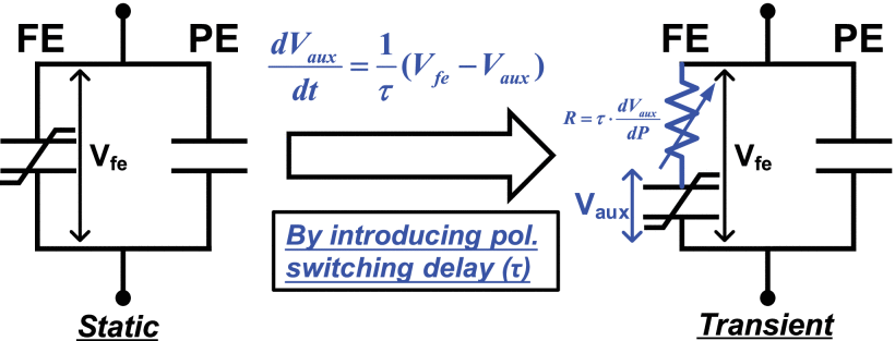
Abstract - We have investigated transient IdVg and IdVd characteristics of ferroelectric field-effect transistor (FeFET) by simulation with ferroelectric model considering polarization switching dynamics. We show transient negative capacitance (TNC) with polarization reversal and depolarization effect can result in sub-60mV/dec subthreshold swing (SS), reverse drain-induced barrier lowering (R-DIBL), and negative differential resistance (NDR) without traversing the quasi-static negative capacitance (QSNC) region of the S-shaped polarization-voltage (PV) predicted by single-domain Landau theory. Moreover, the mechanisms of R-DIBL and NDR based on the TNC theory are discussed in detail. The results demonstrated in this work can be a possible explanation for the mechanism of previously reported negative capacitance field-effect transistor (NCFET) with sub-60mV/dec SS, R-DIBL, and NDR.
Equivalent circuits of a ferroelectric capacitor in both static and transient conditions.

Oct 3, 2019

[paper] Gallium Nitride FET Model

Gallium Nitride FET Model
V V Orlov, G I Zebrev
National Research Nuclear University MEPHI, Moscow, Russia
E-mail: gizebrev@mephi.ru

Abstract: We have presented an analytical physics-based compact model of GaN power FET, which can accurately describe the I-V characteristics in all operation modes. The model considers the source-drain resistance, different interface trap densities and self-heating effects. (read more 
https://arxiv.org/ftp/arxiv/papers/1909/1909.05702.pdf)

Introduction: Gallium nitride (GaN) high electron mobility transistor (HEMT) technology has many advantages, that make it a promising candidate for high-speed power electronics. It allows high-power operation at much higher frequencies than silicon laterally diffused metal-oxide-semiconductor field-effect transistors (LDMOSFETs), currently a staple for the cellular base station industry [1]. The high breakdown voltage capability (over 100 V), high electron mobility, and high-temperature performance of GaN HEMTs are the main factors for its use in power electronics applications. Circuits design in both application regimes requires the accurate compact device models that can describe the non-linear I-V characteristics. The current state-of-the-art GaN power transistor circuit models are mostly empirical in nature and contain a large number of fitting parameters. The source-drain series resistance and self-heating make the compact modeling difficult [2]. Currently available models are not enough accurate to describe the I-V characteristics of power GaN HEMTs in all operation modes. This means, that we need a compact physics-based analytical model based on the physical description of the device. In this paper, we present a physics-based GaN power transistor model based on generic approach The paper contains 3 parts. In the first part, we will give a concise description of the model. The specific power HEMT’s effects, such as series resistance and self-heating will be discussed in the second and third parts 

Apr 24, 2013

TED Call for Papers on Compact Modeling of Emerging Devices

Compact Models (CMs) for circuit simulation have been at the heart of CAD tools for circuit design for almost five decades. As the mainstream CMOS technology is scaled into the nanometer regime, development of a truly physical and predictive CM for circuit simulation that covers geometry, bias, temperature, DC, AC, RF, and noise characteristics becomes a major challenge. The last call for a special issue on “advanced compact models and 45-nm modeling challenges” was in 2005. Seven years have passed, new technology nodes have been implemented, compact models have evolved and new compact models as well as compact models for new devices are being developed. Therefore, there is a need for another special issue dedicated to the advancement and challenges in core field-effect transistor (FET) models for 32-nm technologies and beyond as well as emerging technologies. For the core FET models, the associated noise/mismatch and reliability/variability models as well as proximity effects have become an essential part of the modeling effort. High-frequency, high-voltage, high-power, high-temperature devices have been extensively investigated, and their CMs are being reported in the literature. Device/circuit interaction and layout-dependent proximity effects are also hot topics today that are essential in nanometer chip designs. It is timely to report advances in these CMs in the 32-nm/22-nm technology era.

Concurrently, nonclassical MOSFETs as well as their CMs, such as multigate FinFETs and nanowire FETs, partially/fully-depleted ultrathin body (UTB) SOT, and thin-film transistors (TFTs), have emerged over the past decades. With the announcement of FinFETs being used in 22-nm and sub-22nm technology nodes, the need for such core models for fabless designers becomes an urgent reality. In these nonclassical devices, transistors are essentially short-channel, narrow-width, and thin-body. Tt is also an interesting topic to discuss and debate on the two different formalisms “top-down” drift-diffusion formulation adding ballistic effects versus “bottom-up” quasi-ballistic formulation adding scattering effects for modeling the real devices that are somewhere in between. Heterogeneous integration of various devices into the CMOS platform also becomes an important trend.
In addition, it is also timely to report advances in CMs of emerging devices beyond traditional silicon CMOS, such as different materials (III-V/Ge channel, organic) and different source/drain injection mechanisms (Schottky-barrier, tunneling, and junctionless FETs). These emerging device options for future VLSI building blocks have been studied extensively, while good physical CMs are still lacking. The special issue in these topics will stimulate research and development to promote modeling efforts such that theory would lead and guide technology realization and selection for future generations.
The special issue for the TRANSACTIONS ON ELECTRON DEVICES on compact modeling of emerging devices is devoted to the review and report of advancements in CMs for 32-nm technologies and beyond, including bulk and nonclassical CMOS and their associated noise/mismatch and reliability/variability models, as well as various emerging devices as future generation device options. It is timely as the industry is in the transition from traditional planar bulk-CMOS towards vertical FinFET technologies, and exploration of heterogeneous integration with various materials and structural choices.


Please submit manuscripts by using the following URL: http://mc.manuscriptcentral.com/ted
MAKE SURE TO MENTION THE SPECIAL ISSUE IN THE COVER LETTER

Paper submission Deadline: June 30, 2013
Scheduled Publication Date: February 2014

Guest Editors:
Xing Zhou, Nanyang Technological University, 
Jamal Deen, McMaster University, 
Benjamin Iniguez, Universitat Rovira i Virgili, 
Christian Enz, Swiss Federal Institute of Technology, 
Rafael Rios, Intel Corp.

If you have any questions about submitting a manuscript, please contact:
IEEE EDS Publications Office
445 Hoes Lane Piscataway JN 08854
Phone: +1 732 562 6855

Digital Object Identifier 10.1109/TED.2013.2253418