Showing posts with label ACM. Show all posts

Nov 29, 2023

[paper] Noise modeling for cryogenic applications

Giovani Britton1,2, Salvador Mir2, Estelle Lauga-Larroze2, Benjamin Dormieu1, Quentin Berlingard3,4, Mickael Casse3 and Philippe Galy1
Noise modeling using look-up tables and DC measurements for cryogenic applications.
VLSI-SoC 2023 - 31st IFIP/IEEE International Conference on Very Large Scale Integration,
Oct 2023, Sharjah, United Arab Emirates.
DOI: 10.1109/VLSI-SoC57769.2023.10321896
hal-04305746
1STMicroelectronics, Crolles, France
2Univ. Grenoble Alpes, CNRS, Grenoble-INP, TIMA
3Univ. Grenoble Alpes, CEA, LETI
4Univ. Grenoble Alpes, CNRS, Grenoble-INP, IMEP-LAHC

Abstract 
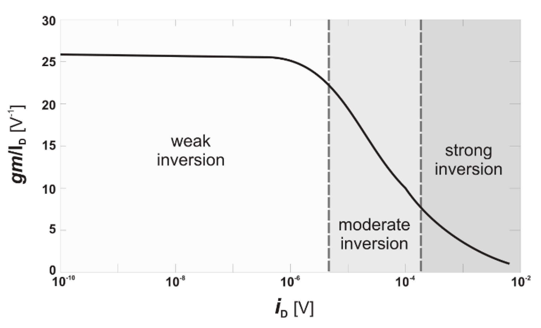
: There is today a lack of mature transistor-level compact models for the simulation of integrated circuits at cryogenic temperatures. This is particularly the case for the simulation of the noise behavior which is critical for most applications. In this paper, we aim at an efficient prediction of the white noise behavior of basic amplifying stages working at RF frequencies and cryogenic temperatures. For this, we propose the use of DC measurements that are incorporated in a LookUp Table (LUT) and fed to a mathematical noise model. We illustrate the approach for the case of a transistor in common source configuration. The results of circuit simulation of the noise parameters in the standard temperature range are very close to the estimation of the same parameters using the LUT with just DC measurements. The approach can be readily extended to the analysis of circuits with multiple components. Next, the LUT approach is used for estimating the noise parameters at cryogenic conditions, considering DC measurements that have been carried out at these temperatures. The paper illustrates the feasibility of carrying out a cryogenic design using a LUT-based approach while accurate compact models are not yet available.

Fig : Measurement data and EKV or ACM generated parameters are added
to the LUT generated by the interface between EDA tools

Acknowledgments : This work was supported by the French program Conventions Industrielles de Formation par la Recherche (CIFRE) and Labex MINOS of French program ANR-10-LABX-55-01.

Dec 23, 2021

[Special Issue] ACM Transactions on Machine Learning for CAD / EDA

ACM Transactions on Design Automation of Electronic Systems
Special Issue on Machine Learning for CAD / EDA 

Guest Editors
• Yibo Lin, Peking University
• Avi Ziv, IBM Research, Haifa, Israel
• Haoxing Ren, NVIDIA Corp.

Advances in Machine Learning (ML) over the past half-dozen years have revolutionized the effectiveness of ML for a variety of applications. However, design processes present challenges that require parallel advances in ML and CAD as compared to traditional ML applications such as image classification. 
This special issue seeks original submission on ML applications to the entire design flow - including ML applications to validation and test. The application of machine learning to mask preparation and layout generation are topics which are seeing very active research recently. ML is also being applied to improve the robustness of integrated circuits and systems. Power and thermal management are probably the most important limiting factors for ICs today - ML-based techniques are being explored to address this bottleneck. All these topics, as well as further potential topics mentioned below, are of interest to this special issue. In addition to submissions from academia, submissions from industry are much welcome. 

Topics of interest to this special issue include, but not limited to, the following:
• ML for system-level design
• ML approaches to logic design and synthesis
• ML for timing
• ML for clock networks and power grids
• ML for variation-aware design, analysis and optimization
• ML for physical design
• ML for analog design
• ML for power and thermal management
• ML for Design Technology Co-Optimization (DTCO)
• ML methods to predict aging and reliability
• Labeled and unlabeled data in ML for CAD
• ML techniques for resource management in many cores
• ML for verification and validation
• ML for test
• ML for library design and optimization 

Important Dates:
• Submissions deadline: February 15, 2022
• First-round review decisions: April 15, 2022
• Deadline for revision submissions: May 15, 2022
• Notification of final decisions: June 15, 2022
• Tentative publication: Summer 2022 

Submission Information: 
Authors are encouraged to submit high-quality original research contributions. Please clearly identify the additional material from any original conference or workshop paper in your submitted manuscript. Submissions should be made through the ACM TODAES submission site (http://mc.manuscriptcentral.com/todaes) and formatted according to TODAES author guidelines at: https://dl.acm.org/journal/todaes/author-guidelines. Select the paper type “Special Issue on Machine Learning for CAD/EDA.” 

For questions and further information, please contact guest editors at:
Avi Ziv

Nov 27, 2021

[paper] Bridging the gap between design and simulation of low voltage CMOS circuits

C. M. Adornes, D. G. Alves Neto, M. C. Schneider and C. Galup-Montoro
Bridging the gap between design and simulation of low voltage CMOS circuits
2021 IEEE Nordic Circuits and Systems Conference (NorCAS), 2021, pp. 1-5,
DOI: 10.1109/NorCAS53631.2021.9599867

Abstract: This work proposes a simplified MOSFET model based on the Advanced Compact MOSFET (ACM) model, which contains only four parameters to assist the designer in understanding how the main MOSFET parameters affect the design. The 4-parameter model was implemented in Verilog-A to simulate different circuits designed with the ACM model. A CMOS inverter and a ring oscillator were designed and simulated, either using the 4-parameter ACM model or the BSIM model. The simulation results demonstrate that the 4-parameter model is very suitable for ultra-low-voltage (ULV) modeling. In the ultra-low-voltage domain, some of the secondary effects of the MOSFET are not relevant and thus not included in the 4-parameter model. A simplified MOSFET model for the ULV domain is of great importance to applications such as energy harvesting, sensor nodes for the Internet of Things, and always-on circuits.

Acknowledgment: The authors would like to thank the Brazilian agencies CAPES, finance code 001, and CNPq for supporting this work.

REF:
[1] A. I. A. Cunha, M. C. Schneider and C. Galup-Montoro, "An MOS Transistor Model for Analog Circuit Design", IEEE J. Solid-State Circuits, vol. 33, no. 10, pp. 1510-1519, October 1998
[2] C. Galup-Montoro and M. C. Schneider, "The compact all-region MOSFET model: theory and applications", IEEE 16th International New Circuits and Systems Conference (NEWCAS), pp. 166-169, June 2018
[3] M. C. Schneider and C. Galup-Montoro, CMOS Analog Design Using All-Region MOSFET Modeling, Cambridge University Press, 2010
[4] C. Galup-Montoro and M. C. Schneider, MOSFET modeling for circuit analysis and design, World Scientific, 2007
[5] Verilog-A Reference Manual, Agilent Technologies, 2004
[6] 0. F. Siebel, "Um modelo eficiente do transistor MOS para o projeto de circuitos VLSI," Universidade Federal de Santa Catarina, Florianopolis, 2007
[7] F. N. Fritsch, R. E. Shafer and W. P. Crowley, "Algorithm 443: Solution of the transcendental equation wew=x," Commun. ACM, vol. 16, no. 2, pp. 123-124, 1973
[8] O. F. Siebel, M. C. Schneider and C. Galup-Montoro, "MOSFET threshold voltage definition, extraction and some applications," Microelectronics Journal, vol. 43, no. 5, pp. 329-336, May 2012
[9] G. Hiblot. DIBL-Compensated Extraction of the Channel Length Modulation Coefficient in MOSFETS. IEEE Transactions on Electron Devices, vol. 65, no. 9, pp. 4015-4018, 2018
[10] BSIM4v4.5.0 Technical Manual, Department of Electrical Engineering and Computer Science, UC Berkeley, Berkeley, CA, USA. 2004
[11] Y. Tsividis and C. McAndrew, Operation and Modeling of the MOS Transistor, Oxford Univ. Press, 2011
[12] J. V. T. Ferreira, C. Galup-Montoro, "Ultra-low-voltage CMOS ring oscillators. Electronics Letters," IET, v. 55, n. 9, p. 523-525,2019
[13] E. M. Camacho-Galeano, C. Galup-Montoro and M. C. Schneider, "A 2-nW 1.1.-V self biased current reference in CMOS technology," IEEE Transactions on Circuits and Systems II: Express Briefs, vol. 52, no. 2, pp. 61-65, 2005
[14] E. Bolzan, E. B. Storck, M. C. Schneider and C. Galup-Montoro, "Design and testing of a CMOS SelfBiased Current Source," 2019 26th IEEE International Conference on Electronics, Circuits and Systems (ICECS), pp. 382-385, 2019

Feb 12, 2021

[paper] ACM) Model in VHDL-AMS

A. S. Kumar, Ch. Rekha, Y. D. S. Raju 
Behavioral Modeling of the Advanced Compact MOSFET (ACM) Model with VHDL-AMS 
OAIJSE, Vol. 6, Issue 1, January 2021 
ISSN (Online) 2456-3293 

*Holymary Institute Of Technology And Science, Bogaram(V), Keesara (M), Hyderabad

Abstract: This paper reports a VHDL-AMS implementation of the Advanced Compact MOSFET (ACM) model. This behavioral model aims at being a reference model for ACM code developers, helping to implement and maintain simulators specic code. Simulation results from classical testbenches are presented and con_rm the correctness of the proposed model.
Fig: The used methodology propose this testbench [ref]

[ref] A. L. T. B. da Fonseca and F. R. de Sousa, "Behavioral modeling of the Advanced Compact MOSFET (ACM) model with VHDL-AMS," 2008 Joint 6th International IEEE Northeast Workshop on Circuits and Systems and TAISA Conference, Montreal, QC, 2008, pp. 169-172
doi: 10.1109/NEWCAS.2008.4606348.

Abstract: This paper reports a VHDL-AMS implementation of the Advanced Compact MOSFET (ACM) model. This behavioral model aims at being a reference model for ACM code developers, helping to implement and maintain simulators specific code. Simulation results from classical testbenches are presented and confirm the correctness of the proposed model.

May 18, 2020

[paper] Novel Design and Optimization and the gm/ID Ratio

A Novel Design and Optimization Approach for Low Noise Amplifiers (LNA) Based on MOST Scattering Parameters and the gm/ID Ratio
1Facultad de Ingeniería, Universidad Católica de Córdoba, Córdoba 5017 (AN)
2Service d’Électronique et Microélectronique, Université de Mons (UMONS), 7000 Mons (BE)
3Departamento de Electrónica, Instituto de Astrofísica de Canarias (IAC), 38200 La Laguna (SP)
* Author to whom correspondence should be addressed.
Electronics 2020, 9(5), 785; https://doi.org/10.3390/electronics9050785
Received: 31 March 2020 / Revised: 30 April 2020 
Accepted: 9 May 2020 / Published: 11 May 2020

AbstractThis work presents a new design methodology for radio frequency (RF) integrated circuits based on a unified analysis of the scattering parameters of the circuit and the gm/ID ratio of the involved transistors. Since the scattering parameters of the circuits are parameterized by means of the physical characteristics of transistors, designers can optimize transistor size and biasing to comply with the circuit specifications given in terms of S-parameters. A complete design of a cascode low noise amplifier (LNA) in 65nm CMOS technology is taken as a case study in order to validate the approach. In addition, this methodology permits the identification of the best trade-off between the minimum noise figure and the maximum gain for the LNA in a very simple way.
Figure: gm/ID versus iD

Acknowledgement - This research was funded by Universidad Católica de Córdoba (Argentina), the Walloon Region DGO6 BEWARE Fellowships Academia Programme (1410164-POHAR, cofunded by the European Marie Curie Actions), the Belgian FNRS (Fond National pour la Recherche Scientifique) and the Argentinean MINCyT (Ministerio de Ciencia y Tecnología).