Showing posts with label JFET. Show all posts

Oct 21, 2021

[paper] Charge-based Modeling of FETs

Jean-Michel Sallese 
Charge-based modeling of field effect transistors, Make it easy
Joint International EUROSOI and EuroSOI-ULIS Workshop (Sept.2020)
DOI: 10.1109/EuroSOI-ULIS53016.2021.956068
 
EDLab, EPFL,  Lausanne  (CH)
 
Abstract: In this presentation, we revisit some charge voltage dependencies for different architectures of field effect transistor, emphasizing on compactness and simplicity while maintaining a close link with physics, which makes these models predictive and accurate for general purposes of compact modeling.

Fig: The gm/I invariant versus the inversion coefficient IC. 
The operation modes of the MOSFET are clearly defined. 

Acknowledgements: I (JMS) would like to thank F. Jazaeri, C. Lallement, W. Grabinski, B. Iniguez and M. Bucher for their constructive interactions. 


Mar 23, 2020

MicroTec: Semiconductor Process and Device Simulator

Software Package for 2D Process and Device Simulation
Version 4.0 for Windows
User’s Manual
Publisher: Siborg Systems Inc
Editor: Michael S. Obrecht

MicroTec allows 2D silicon process modeling including implantation, diffusion and oxidation and 2D steady-state semiconductor device simulation like MOSFET, DMOS, JFET, BJT, IGBT, Schottky, photosensitive devices etc. Although MicroTec is significantly simplified compared to widely available commercial simulators, it nevertheless is a very powerful modeling tool for industrial semiconductor process/device design. In many instances MicroTec outperforms existing commercial tools and it is remarkably robust and easy-to-use.

FIG: MicroTec SibGraf GUI windows


Jul 23, 2019

CODEOCEAN: Charge-Based Modeling of Long-Channel Symmetric Double-Gate Junction FETs

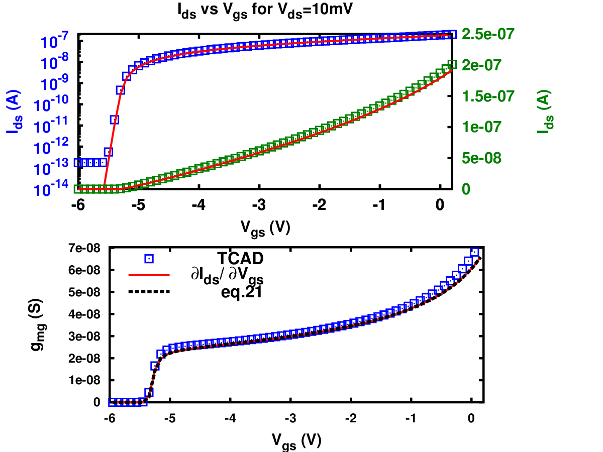
CODEOCEAN capsule written in OCTAVE which calculates the current and transconductances (gm, gmd and gms) using the charge based approach introduced in [1]. The capsule generates graphs demonstrating model versus TCAD simulations. The user can use the capsule code to experiment and reproduce the results in the paper [1]. 
The capsule is provided at the IEEE explorer site under the "Code&Datasets" link. https://ieeexplore.ieee.org/document/8371530 / doi: 10.1109/TED.2018.2838101 
Or at the link below https://codeocean.com/capsule/8244803/tree"

FIG: IdVg and gmVg at Vd=10mV
REF:
[1] N. Makris, F. Jazaeri, J. Sallese, R. K. Sharma and M. Bucher, "Charge-Based Modeling of Long-Channel Symmetric Double-Gate Junction FETs—Part I: Drain Current and Transconductances," in IEEE Transactions on Electron Devices, vol. 65, no. 7, pp. 2744-2750, July 2018.
doi: 10.1109/TED.2018.2838101
Abstract: The double-gate (DG) junction field-effect transistor (JFET) is a classical electron device, with a simple structure that presents many advantages in terms of not only device fabrication but also its operation. The device has been largely used in low-noise applications, but also more recently, in power electronics. Physics-based compact models for JFETs, contrary to MOSFETs, are, however, scarce. In this paper, an analytical, charge-based model is established for the mobile charges, drain current, and transconductances of symmetric DG JFETs, covering all regions of device operation. The model is unified and continuous from subthreshold to linear and saturation operation and is valid over a large temperature range. This charge-based model constitutes the basis of a full compact model of the DG JFET.
Keywords: junction gate field effect transistors;semiconductor device models;mobile charges;double-gate junction field-effect transistor;classical electron device;low-noise applications;power electronics;long-channel symmetric double-gate junction FET;symmetric DG JFET;charge-based modeling;physics-based compact models;drain current;Electric potential;JFETs;Logic gates;Integrated circuit modeling;Junctions;Mathematical model;MOSFET;Analytical model;circuit simulation;compact model;junction field-effect transistor (JFET);temperature effect