Showing posts with label surface potential. Show all posts

Nov 2, 2020

[paper] SPICE Compact Model for Schottky-Barrier FETs

Sheikh Aamir Ahsan, Member, IEEE, Shivendra Kumar Singh, Chandan Yadav, Member, IEEE, Enrique G. Marín, Member, IEEE, Alexander Kloes, Senior Member, IEEE
and Mike Schwarz, Senior Member, IEEE
A Comprehensive Physics-Based Current–Voltage SPICE Compact Model 
for 2-D-Material-Based Top-Contact Bottom-Gated Schottky-Barrier FETs
IEEE Transactions on Electron Devices, vol. 67, no. 11, pp. 5188-5195, Nov. 2020
DOI: 10.1109/TED.2020.3020900

Abstract: In this article, we report the development of a novel physics-based analytical model for explaining the current–voltage relationship in Schottky barrier (SB) 2D material field effect transistors (FETs). The model has at its core the calculation of the surface-potential (SP) which is accomplished by invoking 2-D density of states in conjunction with Fermi–Dirac (FD) distribution for electron and hole statistics. The explicit computation for the SP, carried out using the Lambert-W function together with Halley’s method, is used to construct the SP-based band-diagram for realizing the transparency of the SBs. Thereafter, the ambipolar current is derived in terms of the electron and hole injection phenomena the thermionic emission and Fowler–Nordheim tunneling mechanisms at the SB contacts. Furthermore, drift-diffusion current is derived in terms of the SP and incorporated in the model to account for the scattering in the intrinsic 2D channel. Finally, the Verilog-A model is validated against experimental IV data reported in the literature for two different 2D material systems. This is the first demonstration of an explicit SP-based SPICE model for ambipolar SB-2-D-FETs that is simultaneously built on tunneling-emission and driftdiffusion formalisms.

Fig: (a) Band-diagram sketched along positive y-direction underneath the source electrode. Blue and black lines represent bands before and after applying Vgs. (b) ψ-based diagram sketched along positive x, constructed after calculating ψs and ψd. The geometrical screening length λ is given by λ ≈ (tox t2D)^1/2.

Acknowledgement: This work was supported in part by the National Project Implementation Unit (NPIU) through the third phase of Technical Education Quality Improvement Programme (TEQIP-III) Project and in part by DST-SERB Startup Research Grant under Award SRG/2019/001122.


May 26, 2020

[paper] InAs-OI-Si MOSFET Compact Model

S. K. Maity, A. Haque and S. Pandit
Charge-Based Compact Drain Current Modeling of InAs-OI-Si MOSFET 
Including Subband Energies and Band Nonparabolicity
in IEEE TED, vol. 67, no. 6, pp. 2282-2289, June 2020
doi: 10.1109/TED.2020.2984578

Abstract: In this article, we report a physics-based compact model of drain current for InAs-on-insulator MOSFETs. The quantum confinement effect has been incorporated in the proposed model by solving the 1-D Schrödinger–Poisson equations without using any empirical model parameter. The model accurately captures the variation of surface potential, charge density in the inversion layer, and subband energy levels with gate bias inside the quantum well. The conduction-band nonparabolicity effect on modification in eigen energy, effective mass, and density of states is derived and incorporated into the proposed model. The velocity overshoot effect that originates from the quasi-ballistic nature of carrier transport is also considered in the model. The proposed drain current model has been implemented in Verilog-A to use in the SPICE environment. The model predicted results are in good agreement with the commercial device simulator results and experimental data. 
Fig: Energy band profile of InAs-OI-Si MOSFET in the direction perpendicular to the oxide interface at flat-band condition. E0 and E1 denote the first and the second subband energy levels, respectively, and ΔEc and Vox represent the conduction-band offset between buffer-channel and oxide-channel regions, respectively.

Acknowledgment: The author S. Pandit would like to thank the Department of Electronics and Information Technology, Government of India for utilizing the resources obtained under the SMDP-C2SD Project at the University of Calcutta.

URL: https://ieeexplore.ieee.org/stamp/stamp.jsp?tp=&arnumber=9067014&isnumber=9098120

Jul 23, 2019

[paper] A Surface-Potential-Based Analytical I-V Model of Full-Depletion Single-Gate SOI MOSFETs

1
Department of Electrical and Electronic Teaching, 
College of Information Science and Engineering, 
Huaqiao University, Xiamen 361021, China

2
Department of Electronic Engineering, Jinan University, Guangzhou 510632, China
*
Correspondence: yufei_jnu@126.com; Tel.: +86-0592-6162-385
These two authors contributed equally to this work.

Received: 10 May 2019 / Accepted: 12 June 2019 / Published: 14 July 2019
Electronics 20198(7), 785; https://doi.org/10.3390/electronics8070785

Abstract

: 
A surface-potential-based analytical I-V model of single-gate (SG) silicon-on-insulator (SOI) MOSFETs in full-depletion (FD) mode is proposed and compared with numerical data and Khandelwal’s experimental results. An explicit calculation scheme of surface potential, processing high computation accuracy and efficiency, is demonstrated according to the derivation of the coupling relation between surface potential and back-channel potential. The maximum absolute error decreases into 10−7 V scale, and computation efficiency is improved substantially compared with numerical iteration. Depending on the surface potential, the drain current is derived in closed-form and validated by Khandelwal’s experimental data. High computation accuracy and efficiency suggest that this analytical I-V model displays great promise for SOI device optimizations and circuit simulations.

Keywords:
 silicon-on-insulator MOSFETs; surface potential; back-channel potential; full-depletion; analytical I-V model
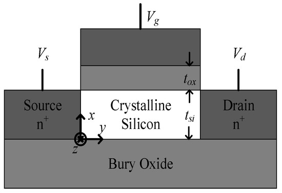
Figure 1. x-y cross section of silicon-on-insulator (SOI) MOSFETs.

Aug 30, 2017

[paper] Surface Potential Equation for Low Effective Mass Channel Common Double-Gate MOSFET

Ananda Sankar Chakraborty and Santanu Mahapatra, Senior Member, IEEE
in IEEE Transactions on Electron Devices
vol. 64, no. 4, pp. 1519-1527, April 2017
doi: 10.1109/TED.2017.2661798

Abstract: Formulation of accurate yet computationally efficient surface potential equation (SPE) is the fundamental step toward developing compact models for low effective mass channel quantum well MOSFETs. In this paper, we propose a new SPE for such devices considering multisubband electron occupancy and oxide thickness asymmetry. Unlike the previous attempts, here, we adopt purely physical modeling approaches (such as without mixing the solutions from finite and infinite potential wells or using any empirical model parameter), while preserving the mathematical complexity almost at the same level. Gate capacitances calculated from the proposed SPE are shown to be in good agreement with numerical device simulation for wide range of channel thickness, effective mass, oxide thickness asymmetry, and bias voltages [read more...]
FIG: Total gate capacitance per unit width Cgg (Vg) for 7-nm-thick device with 100% asymmetry in front and back oxide thicknesses. nmax = 2. Line = model. Symbol = TCAD

Dec 13, 2016

[paper] A surface potential large signal model for AlGaN/GaN HEMTs

A surface potential large signal model for AlGaN/GaN HEMTs
Q. Wu, Y. Xu, Z. Wen, Y. Wang and R. Xu
2016 11th EuMIC, London, UK, 2016, pp. 349-352

doi: 10.1109/EuMIC.2016.7777562

Abstract: This paper presents an accurate analytical surface-potential-based compact model for AlGaN/GaN HEMTs for SPICE-like circuit simulation. Considering the important energy level E0, an easy-implemented analytical continuous expression for the fermi level position Ef was deduced to obtain the surface potential (SP) φs. Then analytical core models for intrinsic charge and drain current are derived based on φs. The model has been implemented in Agilent ADS by using symbolic defined device. Excellent agreement of DC I-V, fundamental output power, power added efficiency and gain is obtained for the first time compared with measurement results. Moreover, the effect of physical parameter such as the barrier thickness d on device characteristic is researched on the basic of this model. The results show that the proposed physical based model can be useful for technological parameters analysis and optimization of process.

[read more: http://ieeexplore.ieee.org/stamp/stamp.jsp?tp=&arnumber=7777562&isnumber=7777458]