Showing posts with label neural network. Show all posts

Jul 19, 2023

[paper] artificial synapse

Md. Hasan Raza Ansari, Udaya Mohanan Kannan, and Nazek El-Atab
Silicon Nanowire Charge Trapping Memory for Energy-Efficient Neuromorphic Computing
IEEE Transactions on Nanotechnology (2023)
DOI 10.1109/TNANO.2023.3296673

SAMA Labs, CEMSE Division, KAUST, Thuwal 23955-6900, Saudi Arabia
Department of Electronic Engineering, Gachon University, Seongnam 13120, Korea

Abstract: This work highlights the utilization of the floating body effect and charge-trapping/de-trapping phenomenon of a Silicon-nanowire (Si-nanowire) charge-trapping memory for an artificial synapse of neuromorphic computing application. Charge trapping/de-trapping in the nitride layer characterizes the long-term potentiation (LTP)/depression (LTD). The accumulation of holes in the potential well achieves short-term potentiation (STP) and controls the transition from STP to LTP. Also, the transition from STP to LTP is analyzed through gate length scaling and high-κ material (Al2O3) for blocking oxide. Furthermore, the conductance values of the device are utilized for system-level simulation. System-level hardware parameters of a convolutional neural network (CNN) for inference applications are evaluated and compared to a static random-access memory (SRAM) device and charge-trapping memory. The results confirm that the Si-nanowire transistor with better gate controllability has a high retention time for LTP states, consumes low power, and archives better accuracy (91.27%). These results make the device suitable for low-power neuromorphic applications.


FIG: Schematic representation of biological and Si-nanowire charge trapping memory as an artificial synapse

Jan 18, 2023

Neural networks and machine learning approach for compact modeling

[NN] Wang, Qiuwei, Mao Ye, Yao Li, Xiaoxiao Zheng, Jiaji He, Jun Du, and Yiqiang Zhao. "MOSFET modeling of 0.18 μm CMOS technology at 4.2 K using BP neural network." Microelectronics Journal (2023): 105678. DOI: 10.1016/j.sse.2022.108580

Highlights
  • The cryogenic characterization of SMIC CMOS technology at 4.2K is presented.
  • An optimization model VCCS is proposed to calibrate the cryogenic characteristics.
  • BP neural network is, for the first time, used in MOSFET modeling.
  • The cryo-model can be applied to SPICE simulator and assist in cryo-CMOS circuit design and simulation.
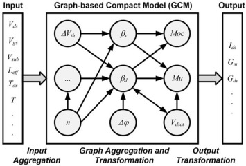
Fig: The structure of graph-based compact model of FinFET. The model receives the input features such as voltages, geometries, etc. as a vector and predicts the drain current (Ids) and its derivatives as output features.


[ML] Gaidhane, Amol D., Ziyao Yang, and Yu Cao. "Graph-based Compact Modeling (GCM) of CMOS transistors for efficient parameter extraction: A machine learning approach." Solid-State Electronics (2023): 108580.

Highlights
  • Developed a Graph-based compact model for FinFET.
  • Model implemented in Verilog-A for SPICE simulation.
  • Requires less number of model parameters and is computationally efficient than BSIM

Oct 4, 2021

Memory for Synaptic Operations

Md. Hasan Raza Ansari, Udaya Mohanan Kannan and Seongjae Cho 
Core-Shell Dual-Gate Nanowire Charge-Trap Memory
for Synaptic Operations for Neuromorphic Applications
Nanomaterials 2021, 11, 1773
DOI 10.3390/nano11071773
 
Graduate School of IT Convergence Engineering, Gachon University, Seongnam 13120, Korea;
 
Abstract: This work showcases the physical insights of a core-shell dual-gate (CSDG) nanowire transistor as an artificial synaptic device with short/long-term potentiation and long-term depression (LTD) operation. Short-term potentiation (STP) is a temporary potentiation of a neural network, and it can be transformed into long-term potentiation (LTP) through repetitive stimulus. In this work, floating body effects and charge trapping are utilized to show the transition from STP to LTP while de-trapping the holes from the nitride layer shows the LTD operation. Furthermore, linearity and symmetry in conductance are achieved through optimal device design and biases. In a system-level simulation, with CSDG nanowire transistor a recognition accuracy of up to 92.28% is obtained in the Modified National Institute of Standards and Technology (MNIST) pattern recognition task. Complementary metal-oxide-semiconductor (CMOS) compatibility and high recognition accuracy makes the CSDG nanowire transistor a promising candidate for the implementation of neuromorphic hardware.
Fig: Schematic representation of biological synapse and 2D representation of CSDG nanowire transistor for artificial synapse device.

Acknowledgement: This research was supported by the National Research Foundation of Korea (NRF) funded by the Ministry of Science and ICT (MSIT) (No. 2016M3A7B4910348, Nano-Material Technology Development Program, 50%) and was partly supported by Institute of Information & Communications Technology Planning & Evaluation (IITP) grant funded by the Korean government (MSIT) (No. 2020-0-01294, Development of IoT based edge computing ultra-low power artificial intelligent processor, 50%).

[see also] M. H. R. Ansari, S. Cho, J.-H. Lee, and B.-G. Park, “Core-Shell Dual-Gate Nanowire Memory as a Synaptic Device for Neuromorphic Application,” IEEE Journal of the Electron Devices Society, pp. 1–1, 2021. DOI: 10.1109/JEDS.2021.3111343


Nov 24, 2020

[paper] Compact Models for Sizing Based on ANN

Husni Habal, Dobroslav Tsonev, Matthias Schweikardt 
Compact Models for Initial MOSFET Sizing Based on Higher-order Artificial Neural Networks
ACM/IEEE Workshop on Machine Learning for CAD (MLCAD ’20)
Nov. 16–20, 2020, Virtual Event, Iceland. ACM, pp. 111-116
DOI: 10.1145/3380446.3430632
1Infineon Technologies AG Munich, Germany
2LogiqWorks Ltd. Sofia, Bulgaria
3Reutlingen University Reutlingen, Germany


Abstract: Simple MOSFET models intended for hand analysis are inaccurate in deep sub-micrometer process technologies and in the moderate inversion region of device operation. Accurate models, such as BSIM6 model, are too complex for use in hand analysis and are intended for circuit simulators. Artificial neural networks (ANNs) are efficient at capturing both linear and non-linear multivariate relationships. In this work, a straightforward modeling technique is presented using ANNs to replace the BSIM model equations. Existing open-source libraries are used to quickly build models with error rates generally below 3%. When combined with a novel approach, such as the gm/Id systematic design method, the presented models are sufficiently accurate for use in the initial sizing of analog circuit components without simulation.

FIG
Figure: ANN Model Architecture.