Showing posts with label DRAM. Show all posts

May 3, 2024

[paper] Compact Model of IDG BEOL Transistor for Capacitorless Memory

Lihua Xu, Kaifei Chen, Zhi Li, Yue Zhao, Lingfei Wang and Ling LiPhysics-Based 
Compact Model of Independent Dual-Gate BEOL-Transistors
for Reliable Capacitorless Memory
in IEEE Journal of the Electron Devices Society
DOI: 10.1109/JEDS.2024.3393418  

School of Microelectronics, University of Science and Technology of China, Hefei (CN)
State Key Lab of FTIC, Institute of Microelectronics of Chinese Academy of Sciences, Beijing (CN)
University of Chinese Academy of Sciences, Beijing (CN)


Abstract: Capacitorless DRAM architectures based on Back End-of-Line (BEOL)-transistors are promising for long retention, high-density and low-power 3D DRAM solutions due to its low leakage, operational flexibility, and monolithic integration capability. Different from classical silicon-based devices, in-depth studies on the performances of nanoscale multi gate transistors (e.g., a-InGaZnO-FET) are still barely conducted for physical description, due to the complicated multi-gating principle, finite-size effects on transport, increased variation sources and enlarged parasitic effect. Hence, high-performance multi-nanoscale (down to ~ 50 nm) dual-gate a-IGZO transistors are fabricated, and a physical compact model is developed based on the surface potential for dual-gated coupling and the disordered transport with finite-size-correction. The short channel behaviors on sub-threshold swing, mobility and threshold voltage are investigated, and contact effects are validated by the transfer-line method (TLM). Regarding the specific challenge of dual-gate alignment, possible misalignment and parasitic effects on multi-device fluctuations are important of large-scale circuit design and analyzed by TCAD simulations. Besides, the bias-temperature instability (BTI) has been comprehensively investigated. In awareness of the above effects, this model bridges fabrication-based material properties and structural parameters, assisting in a threshold fluctuation resistant operation scheme for capacitorless multi-bit memory, showing a great potential in future monolithic integration circuit design using BEOL-transistor.

Fig: (a) Schematic illustration of the IDG a-IGZO FETs with a thickness of ~5nm. (b) Agreement between analytical and numerical results of back gate surface potentials at different VDS with errors in the inset. VTG & VBG denotes DG synchronized-sweep with the same voltage.

Acknowledgements: This work was supported in part by National key research and development program (Grant Nos. 2021YFB3600704), the National Natural Science Foundation of China (Grant Nos. 62274178, 92264204), CAS Interdisciplinary Innovation Team [JCTD-2022-07].




Mar 31, 2021

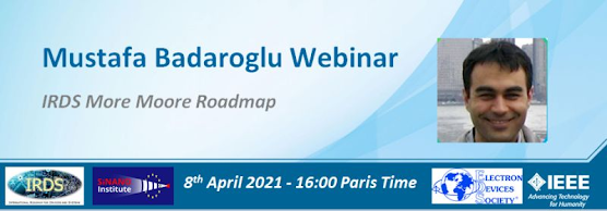
[webinar] "More Moore Roadmap" by IRDS and SINANO


IEEE EDS France, IRDS and the SINANO Institute will organize a Webinar 

"More Moore Roadmap"
by Mustafa Badaroglu 
IRDS-IFT More Moore Leader

The webinar will be held on 8th April 2021 at 16:00 Paris time. Interest participants please register via IEEE vTools by the following link: https://events.vtools.ieee.org/event/register/267103

Other Webinars of the IRDS Chapters will be announced in the EDS Newsletters

Jul 2, 2020

[paper] 1T-1C Dynamic Random Access Memory

1T-1C Dynamic Random Access Memory: 
Status, Challenges, and Prospects 
Alessio Spessot and Hyungrock Oh 
(Invited Paper)
IEEE TED, 67(4), 1382–1393
DOI:10.1109/ted.2020.2963911 

Abstract: This article reviews the status, the challenges, and the perspective of 1T-1C dynamic random access memory (DRAM) chip. The basic principles of the DRAM are presented, introducing the key functional aspects and the structure of modern devices. We present the most relevant historical trends for different modules of the memory chip, such as access device and storage element, reviewing some of the technological challenges faced by industry to guarantee the device shrinking imposed by the economic law. The most recent solutions introduced by the industry in modern DRAM devices for the critical elements are presented. Finally, a survey of the most critical bottleneck for future development is presented, reviewing some of the potential trends and perspectives of DRAM development.

Fig: Review of the historical evolution trend for the cell access device. Various cell access device options are shown. The 4F2 is enabled by the vertical channel. Corresponding technology nodes are included. 

Acknowledgment: The authors would like to thank the imec Core Partners Program for the support. They would also like to thank N. Horiguchi, A. Furnemont, M. H. Na, E. Dentoni Litta, R. Ritzenthaler, and M. Popovici from imec, P. Fazan and C. Mouli from Micron, and C. Kim, Y. Son, and Y. Ji from SK Hynix for the interesting discussions.

May 5, 2020

[paper] Memory Technology – A Primer for Material Scientists.

Schenk, Tony, Milan Pesic, Stefan Slesazeck, Uwe Schroeder, and Thomas Mikolajick
Memory Technology–A Primer for Material Scientists
Reports on Progress in Physics (2020)

Abstract - From our own experience in the group, we know that there is quite a gap to bridge between scientists focused on basic material research and their counterparts in a close-to-application community focused on identifying and solving final technological and engineering challenges. In this review, we try to provide an easy-to-grasp introduction to the field of memory technology for materials scientists. As an understanding of the big picture is vital, we first provide an overview about the development and architecture of memories as part of a computer and point out some basic limitations that all memories are subject to. As any new technology has to compete with mature existing solutions on the market, today's mainstream memories are explained and the need for future solutions is highlighted. The most prominent contenders in the field of emerging memories are introduced and major challenges on their way to commercialization are elucidated. Based on these discussions, we derive some predictions for the memory market to conclude the paper.

TABLE OF CONTENTS
1. INTRODUCTION
2. OVERVIEW AND BASIC LIMITATIONS
3. COMMERCIALLY AVAILABLE MAINSTREAM MEMORIES

3.1. Static and Dynamic Random Access Memory (SRAM/DRAM)
3.2. Flash Memory and Solid-State Drive (SSD)
3.3. Magnetic Hard Disk Drives (HDD) and Magnetic Tapes
3.4. Outlook: Market Trends and Drivers
4. EMERGING MEMORIES
4.1. Resistance-based Read-out: Memory Concepts and Basic Considerations
4.2. Anion migration or valence change memory (VCM)
4.3. Cation migration or electrochemical metallization memory (ECM)
4.4. Phase change memory (PCM)
4.5. Magnetoresistive memory (MRM)
4.6. Ferroelectric Memory (FEM)
4.7. Miscellaneous
5. SUMMARY AND CONCLUSION

FIG: Evolution of the mainstream solutions for the respective memories classes. The introduction of Flash memory partially bridged a technology gap around the year 2009. Today, two types of so-called storage-class memories – a memory-type SCM (SCM 1) and a storage-type SCM (SCM 2) – were proposed to overcome the memory gap. NAND flash already fulfills the role of a mainstream SCM 2. For SCM 1, 3D XPoint could be a promising candidate, but is not a dominant mainstream memory. In future, we will likely see different types of SCMs and NV-RAM with different specifications as required by the respective application – because in the end, the overall system cost decides about the choice of the memory.