Jul 1, 2025

[mos-ak] [OpenPDK] IHP Analog Academy

IHP Analog Academy


We, IHP Analog Academy, are excited to present this deep dive into analog, RF, and mixed-signal IC design, powered by open-source FOSS CAD/EDA tools and the IHP Open PDK.

This hands-on course is designed for engineers, researchers, and students eager to gain practical experience with the SG13G2 process at the 130nm technology node. Originally hosted on-site at IHP in Frankfurt (Oder), participants spent five intensive days exploring everything from fundamental analog simulation to advanced RF, 3D EM modeling, and mixed-signal integration. And now we're excited to release it to the open-source community!

The course covers:
- Bandgap reference design and simulation using the gm/Id methodology
- RF design of a 50 GHz Medium Power Amplifier with EM simulation
- Mixed-signal integration and verification of an 8-bit SAR ADC

Each module emphasizes a real-world design flow using tools like:
ngspice, Xyce, KLayout, OpenEMS, QUCS, and Python for data analysis.

Over time, we will expand the repository with:
- More modules
- Updated toolchain support
- Improvements to existing flows

Explore the IHP Open PDK:
- Open PDK GitHub Repository https://github.com/IHP-GmbH/IHP-Open-PDK 
- Interactive Help via ChatGPT https://chat.openai.com

Note: This is not an introductory IC design course. A basic understanding of electronics and microelectronics is assumed. We're proud to contribute this initiative to the community to help lower the barrier to IC design using open-source tools. We encourage contributions via GitHub Issues or Pull Requests! Your feedback and contributions, are welcome!

Lead Author: Phillip Ferreira Baade-Pedersen
Co-Author: Christian Wittke

The Development of this course is funded by the public German project FMD-QNC (16ME083) from BMFTR (Federal Ministry of Research, Technology and Space / Bundesministerium für Forschung, Technologie und Raumfahrt): https://www.elektronikforschung.de/projekte/fmd-qnc

#opensource #analog #mixedsignal #rf #design

Compact MOSFET Mechanical Stress Model

Bonev, Nikolay, Dirk Michael Nuernbergk, and Christian Lang
Inclusion of Mechanical Stress Effects in a Compact MOSFET Model
Science and Technology 28, no. 2 (2025): 138-149.
DOI: 10.59277/ROMJIST.2025.2.02

1 Melexis Bulgaria EOOD, Sofia, Bulgaria
2 Melexis GmbH Erfurt, Erfurt, Germany

Abstract: The analog performance of integrated circuits relies on stable parameters of its transistors. Mechanical stress changes the electronic properties of silicon and, therefore, also the device parameters. For circuit design, a good model of these effects is needed for a predictable and reliable function of the circuits. This article extracts the changes of various MOSFET parameters under effect of mechanical stress. A compact description of the stress effects is derived by applying tensors of piezo coefficients. The deviations are included in the physically based compact EKV model. A comparison with measured data shows that the stress effects are modelled correctly within a 10 % error margin.

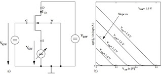
Fig: Extraction setup for the specific current Is


Jun 21, 2025

Technical Lecture - the Celebration of FET100


You are all invited to register and attend the Technical Talks being organized by 
IEEE Electron Device Society (EDS) Delhi Chapter – India and IEEE EDS Community Engagement Ad-hoc Committee 
along with The National Academy of Sciences, India-Delhi Chapter; 
Science Foundation Committee of Deen Dayal Upadhyaya College, University of Delhi, New Delhi, INDIA

Kindly register for each talk separately and forward the email to your students and other colleagues.

Technical Lecture on June 23, 2025 @ 03:00 pm Italy time (GMT +2) i.e. 06:30 pm India Time (GMT +5.30)
The Field Effect Transistor - Evolution of the Modeling ApproachesMassimo Rudan, Professor EmeritusIEEE Life FellowDepartment DEI, University of BolognaSchool of Engineering, Bologna, Italy

Technical Lecture on June 25, 2025 @ 12:00 pm Aachen, North Rhine-Westphalia, Germany (GMT +2) i.e. 03:30 pm India Time (GMT +5.30).
A Brief History of Device Simulation for MOSFETsChristoph JungemannRWTH Aachen University

Technical Lecture on June 27, 2025 @ 02:00 pm (GMT+2) Time in Stockholm, Sweden i.e. 05:30 pm (GMT + 5:30) Indian Standard Time
Efficient Semiconductor Devices for a Sustainable FutureProfessor Mikael Östling, KTH Royal Institute of Technology, FIEEESchool of EECS, Stockholm, Sweden

Technical Lecture on June 30, 2025 @ 04:30 pm CET (GMT+2) Time in Madrid, Spain which shall be 08:00 pm Indian Standard Time (GMT +05:30)
History, evolution and perspective of Thin Film Transistor technologiesBenjamin IñiguezUniversitat Rovira i VirgiliTarragona, Spain

Technical Lecture on July 01, 2025 @ 09:00 am your time (GMT - 5) i.e. 07:30 PM Indian Standard Time (GMT +5:30)
Moore's Law and Radiation Effects on MicroelectronicsDaniel M FleetwoodOlin H. Landreth Professor of Engineering, Professor of Electrical and Computer Engineering, Professor of PhysicsVanderbilt University

Technical Lecture on July 01, 2025 @ 10:00 am (UTC - 5) i.e. 08:30 PM Indian Standard Time (GMT +5:30)
Perovskites – The New Frontier for Solar Photovoltaic Energy Conversion: Science and TechnologyVikram DalalFellow: IEEE, APS, AAASAnson Marston Distinguished ProfessorIowa State University, USA

Technical Lecture on 
July 2, 2025 @ 4:00 pm Italy time (GMT +2) i.e. 07:30 PM Indian Standard Time (GMT +5:30)
Nanoelectronics and Nanosystems Device Engineering for Sustainability, in the Energy and Variability Efficiency(E.V.E.) EraSimon Deleonibus, Life Fellow IEEE, Emeritus Fellow Electrochemical Society, Alternatives, Laboratoire d'Electronique et des Technologies de l'Information,(CEA-LETI), Grenoble, France.

Technical Lecture on
July 3, 2025 @ 10:30 am Italy time (GMT - 4) i.e. 08:00 PM Indian Standard Time (GMT +5:30)
Spin-field effect transistor – the unusual FETSupriyo Bandyopadhyay, Dept. of Electrical and Computer Engineering, Virginia Commonwealth University, Richmond, VA 23284

-- with regards -- Manoj Saxena

Professor Manoj Saxena | आचार्य मनोज  सक्सेना 
FNASc(IN), FIETE(IN), SMIEEE(USA)
Department of Electronics | इलेक्ट्रॉनिक्स विभाग
Deen Dayal Upadhyaya College | दीन दयाल उपाध्याय कॉलेज
University of Delhi | दिल्ली विश्वविद्यालय
Dwarka Sector-3, New Delhi-110078 | द्वारका क्षेत्र -, नई दिल्ली -११००७८
India | भारत

Jun 20, 2025

[C4P] Micro Nano & Chips Tech 2025

 
12th International Conference on Micro-Nano & Chips Tech
https://2025.micro-nano.gr

Dear Colleagues,

We are pleased to invite you to participate in  MICRO NANO & CHIPS TECH 2025, the 12th International Conference on Micro-Nanoelectronics, Nanotechnology, and MEMS, which will be held from  November 6–9, 2025, at the  Cultural Center of Chania, Crete, Greece.

Due to numerous requests during the summer vacation, we are pleased to announce that the paper submission deadline has been extended to 

September 5th!


For details on topics, submission guidelines, and registration, please visit the official conference website.


Explore our updated list of  Plenary and Invited Speakers  

  • Dr. George Kotrotsios: CSEM (ret.), Vice President HCCC
  • Prof. Christian Enz: EPFL (ret.)
  • Dr. Maria Farsari: Research Director at IESL/FORTH
  • Prof. Spiros H. Anastasiadis: Department of Chemistry, University of Crete; former Director of IESL/FORTH
  • Prof. Emmanouil Kriezis: School of Electrical and Computer Engineering, Aristotle University of Thessaloniki
  • Dr. Maria Farsari: Research Director at IESL/FORTH

For more information, please visit the conference website:  https://2025.micro-nano.gr/  


Jun 12, 2025

[mos-ak] [Media Note] MOS-AK INAOE Workshop, Puebla (MX)

MOS-AK INAOE Workshop on Semiconductor Technologies
Puebla (MX), May 14-16, 2025

Media Note

The MOS-AK Workshop on Semiconductor Technologies was held at the Instituto Nacional de Astrofísica, Óptica y Electrónica (INAOE) in Tonantzintla, Puebla, México, on May 14-16, 2025. This workshop was sponsored by MOS-AK, the INAOE, and IEEE through the Puebla Section and the local chapters for the Electron Devices and Instrumentation and Measurements societies. The MOS-AK event was inaugurated by Dr. Wladek Grabinski representing MOS-AK and IHP; Dr. David Sánchez, INAOE's General Director, Dr. Claudia Feregrino, Director of Research and Development for INAOE, and Dr. Roberto Murphy, the local organizer.

The objective of the workshop was to present the various open source tools for the design and simulation of integrated circuits (ICs). It consisted of in person as well as remote keynote speeches by experts in the field, and of a three-hour workshop on digital design synthesis.

The opening talk was by Dr. Wladek Grabinski (MOS-AK), covering a description of all the available FOSS CAD/EDA tools and programs for the design, simulation and fabrication of ICs using OpenPDK. This was a very enlightening run-through of the opportunities that can be exploited by all those who work in the field, at all levels. 

It was followed by a conference by Dr. Joaquín Faneca Ruedas, from the Centro Nacional de Microelectrónica (CNM) in Barcelona, Spain. He spoke about silicon nitride photonics, which is fast becoming a scalable platform for integrated optics. We then had the pleasure of listening to Dr. Medhi Saligane talk on agent AI for analog layout generation. Dr. Saligane is now with Brown University in the US. The first day was closed by a talk on memristor modeling by Dr. Arturo Sarmiento from INAOE. Memristors are fast becoming a common element in IC design, and their modeling and eventual characterization has become a very important field of endeavor in recent years.

The second day was opened by Dr. Colin Shaw from Silvaco (US) who gave a deep description of the status of the Si2 Compact Model Coalition.
The rest of the morning was dedicated to a three-hour workshop on digital circuit synthesis using open source CAD/EDA design tools.

Friday's first talk was by Dr. Harriet Parnell, a senior academic engineer at Ansys, and who gave a talk describing Ansys Lumerical FDTD tool, with a case study of a nanohole array. This was followed by a description of logic technology device innovations, given by Dr. Carlos Díaz, the Senior Director for Research and Development for Taiwan Semiconductor Manufacturing Company (TSMC). This great talk was followed by a presentation of the MOSbius project given by Dr. Peter Kinget, the Bernard J. Lechner Professor of Electrical Engineering at Columbia University. The workshop was closed by a researcher at INAOE, Dr. Reydezel Torres, who spoke of the simulation of chip-to-chip interconnects, another very important aspect of semiconductor technology.

The MOS-AK INAOE workshop was attended by 86 participants, mostly undergrad students but also by professional academicians and scientists. We can call it a success, and we hope that it has contributed to the country's much-needed progress in integrated circuit design and technology.

-- R.Murphy and W.Grabinski 
-- on the behalf of the MOS-AK INAOE Organizing Committee

Enabling Compact Modeling R&D Exchange

RM/WG120625