Sep 30, 2021

[SEMI Press Release] SEMI Applauds European Chips Act, Aimed at Boosting Semiconductor R&D and Manufacturing https://t.co/WZOd8Sw5Sh #Europe #research #development #semiconductors  #manufacturing #publicpolicy #semi #chip #EU https://t.co/mHGUZkRaXY


from Twitter https://twitter.com/wladek60

September 30, 2021 at 08:31PM
via IFTTT

[paper] New Design Concept for the IoT Era

Pedro Toledo, Graduate Student Member, IEEE, Roberto Rubino, Graduate Student Member, IEEE, Francesco Musolino, Member, IEEE, and Paolo Crovetti, Senior Member, IEEE
Re-Thinking Analog Integrated Circuits in Digital Terms: A New Design Concept for the IoT Era
IEEE Transactions on Circuits and Systems—II: Express Briefs, 
Vol. 68, No. 3, March 2021
DOI:  10.1109/TCSII.2021.3049680

* DET, Politecnico di Torino (IT)

Abstract: A steady trend towards the design of mostly-digital and digital-friendly analog circuits, suitable to integration in mainstream nanoscale CMOS by a highly automated design flow, has been observed in the last years to address the requirements of the emerging Internet of Things (IoT) applications. In this context, this tutorial brief presents an overview of concepts and design methodologies that emerged in the last decade, aimed to the implementation of analog circuits like Operational Transconductance Amplifiers, Voltage References and Data Converters by digital circuits. The current design challenges and application scenarios as well as the future perspectives and opportunities in the field of digital-based analog processing are finally discussed.
Fig: a) Kuijk’s Bandgap voltage reference [i]. b) Microcontroller-based proof
of concept prototype.
REF:
[i] K. E. Kuijk, “A precision reference voltage source,” IEEE J. Solid-StateCircuits, vol. SSC-8, no. 3, pp. 222–226, Jun. 1973.

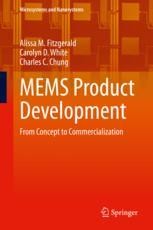
[book] MEMS Product Development

Fitzgerald, Alissa M., Chung, Charles C.
MEMS Product Development: From Concept to Commercialization
ISBN 978-3-030-61709-7

Drawing on their experiences in successfully executing hundreds of MEMS development projects, the authors present the first practical guide to navigating the technical and business challenges of MEMS product development, from the initial concept stage all the way to commercialization. The strategies and tactics presented, when practiced diligently, can shorten development timelines, help avoid common pitfalls, and improve the odds of success, especially when resources are limited. MEMS Product Development illuminates what it really takes to develop a novel MEMS product so that innovators, designers, entrepreneurs, product managers, investors, and executives may properly prepare their companies to succeed.


Table of contents (20 chapters)
  1. The Opportunities and Challenges of MEMS Product Development, pp. 3-8
  2. Economics of Semiconductor Device Manufacturing and Impacts on MEMS Product Development, pp. 9-16
  3. Stages of MEMS Product Development, pp. 17-28
  4. What Is the Product? Requirements Analysis, pp. 31-45
  5. Is There a Business Opportunity? Product Unit Cost Modeling, pp. 47-57
  6. What Is the Budget for Development?, pp. 59-70
  7. Leveraging Third-Party Intellectual Property to Accelerate Product Development, pp. 71-79
  8. Organization Planning for Successful Development, pp. 81-92
  9. The MEMS Product: Functional Partitioning and Integration, pp. 95-110
  10. Starting a New MEMS Device Design, pp. 111-127
  11. Design for Manufacturing: Process Integration and Photomask Layout, pp. 129-148
  12. Design for Back-end-of-Line Processes, pp. 149-156
  13. Strategies for Codevelopment of the Electronics and Package, pp. 157-166
  14. Planning a Development Test Program, pp. 167-183
  15. Risk Mitigation Strategies for Prototype Fabrication, pp. 185-195
  16. Documenting MEMS Product Technology for Transfer to Manufacturing, pp. 197-211
  17. Determining Readiness for Volume Production, pp. 215-222
  18. Selecting a Foundry Partner, pp. 223-239
  19. Transferring Technology for Production, pp. 241-252
  20. Manufacturing Test: Opportunity, Cost, and Managing Risk, pp. 253-268

Sep 29, 2021

[mos-ak] [online publications] 18th MOS-AK ESSDERC/ESSCIRC Workshop Grenoble; Sept. 6, 2021


The MOS-AK Association with local technical program promoters and the International MOS-AK Board of R&D Advisers as well as all the Extended MOS-AK TPC Committee have organized its subsequent 18th MOS-AK ESSDERC/ESSCIRC Workshop as a virtual/online event on Sept.6, 2021

Online Publications:
There are MOS-AK technical presentations covering selected aspects of the compact/SPICE modeling and its Verilog-A standardization; see all the slide presentations online at corresponding link:
The MOS-AK Association plans to continue its standardization efforts by organizing future compact modeling meetings, workshops and courses around the globe later this year and thru the next 2022 year, including:
  • 14th US MOS-AK Workshop, Silicon Valley (US) Dec. 2021
    • in timeframe of IEDM and Q4 CMC Meetings
  • 4th MOS-AK at LAEDC Workshop, Mexico 2022
W.Grabinski on the behalf of International MOS-AK Committee
WG29092021
 

Sep 27, 2021

[paper] Degradations in LDMOS Transistors

Yen-Pu Chen1, Bikram K. Mahajan1, Dhanoop Varghese2, Srikanth Krishnan2, Vijay Reddy2
and Muhammad A. Alam1
Three-point I–V spectroscopy deconvolves region-specific degradations in LDMOS transistors
Appl. Phys. Lett. 119, 122102 (2021); 
DOI: 10.1063/5.0058477

1 Department of ECE, Purdue University, West Lafayette, Indiana 47906, USA
2 Texas Instruments Inc., Dallas, Texas 75043, USA

Abstract: Unlike traditional logic transistors, hot carrier degradation (HCD) in power transistors involves simultaneous and potentially correlated degradation in multiple regions. One must deconvolve and characterize the voltage- and temperature-dependence of these region-specific degradations to develop a predictive HCD model of power transistors. Unfortunately, power transistors' doping and geometrical complexities make it challenging to use traditional defect-profiling techniques, such as charge-pumping or gated-diode methods. This Letter uses a physics-based tandem-FET model of Laterally Diffused MOS (LDMOS) transistors to develop a “three-point I–V spectroscopy” technique that uses the time-evolution of three critical points of the measured I–V characteristics to extract mobility and threshold voltage degradations in the channel and drift regions. This innovative approach should generalize to other configurations of the LDMOS transistor as well.

Fig: The proposed tandem-FET compact model. The channel (ch) and the drift (dr) regions function individually as a MOSFET with different 𝑉th and dimensions. Three adjustable degradation parameters are 𝛥𝜇𝑐ℎ, 𝛥𝑉𝑐ℎth, and 𝛥𝜇𝑑𝑟.

Acknowledgements: Y.-P.C and B.K.M contributed equally to this work. The authors gratefully acknowledge the access to the characterization facilities at Birck Nanotechnology Center, Purdue University, for the results presented in this article.