Nov 11, 2022

Fwd: Last Call: ECS 2023 - Boston


243rd ECS Meeting – Boston, May 28 – June 2, 2023

"H02 - Advanced CMOS-Compatible Semiconductor Devices 20"


Abstract Submission Deadline (750 words = 1 page): December 1, 2022

You can also use a single "Image Upload" to include Image, figures, equations, tables if necessary.


Abstract submissionhttps://ecs.confex.com/ecs/243/cfp.cgi

Do not forget to select H02 symposium for submission…


Full text manuscript: The authors of accepted abstracts should submit the full text manuscript for the ECS Transactions no later than March 16, 2023.


This symposium focuses on studies of new devices, circuits and applications for Moore and More-than-Moore technology, including:


I. More-Moore technology contributing to the semiconductor industry

(a) CMOS compatible devices, circuits and applications:

·        SOI devices, advanced Bulk MOSFETs, scaled devices and simulations;

·        Multi-gate devices (FinFET, triple gate, nanowire, nanosheet), Junctionless FET;

·        high-power devices, semiconductor sensors, Tunnel-FET devices, memory devices;

(b) Device physics and process technology using new materials for noise issues of devices and circuits;

(c) Space applications including low-temperature electronics and radiation hardness

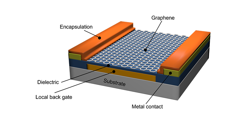
(d) CMOS co-integration of 2D materials (TMDs, etc.)

(e) Self-heating and reliability of scaled MOSFET

(f) Devices with high mobility materials, advanced gate stack


II. More-than-Moore technology

(a) New MEMS applications

(b) Carbon-nanotube and 2D device applications

(c) Sensing applications: Health, environment and security.

(d) Advanced packaging

(e) 2.5D/3D stacking integration

(f) Advanced material and device for Memory, Analog/RF and HV applications


Symposium Organizers:

*Joao Martino (Lead organizer)University of Sao Paulo, Brazil, email: martino@usp.br

*Jean-Pierre Raskin, Universite Catholique de Louvain, Belgium, email:  jean-pierre.raskin@uclouvain.be

*Siegfried Selberherr, TU Wien, Austria, email: Selberherr@TUWien.ac.at

*Hiromu Ishii, Toyohashi University of Technology, Japan, email: ishii@ee.tut.ac.jp

*Francisco Gamiz, Universidad de Granada, Spain, email: fgamiz@ugr.es

*Bich-Yen Nguyen, Soitec, USA, email: Bich-yen.Nguyen@soitec.com

*Eddy Simoen, Imec, Belgium, email: eddy.simoen@ugent.be

 ----------------------------------------

Confirmed INVITED SPEAKERS in alphabetic order by first name:


[1] Dra Bernardette Kunert (Imec, Belgium)

"III-V on Si technologies for 6G electronics"

[2] Prof. Bogdan Cretu (Ensicaen, Caen, France)

"In-deep DC and low frequency noise characterization of double nanosheet FETs DC at room and cryogenic temperatures"

[3] Prof. Cor Claeys (KU Leuven, Leuven, Belgium) – Keynote Speaker

"Technological Challenges and Emerging Device Architectures for Future Semiconductor Micro and Nanoelectronics"

[4] Profa. Cristell Maneux (University of Bordeaux, France)

"RF and mmW technologies"

[5] Prof. Jose Alexandre Diniz (UNICAMP, Brazil)

"ISFET-based Sensors"

[6] Dr. Koen Martens (Imec, Belgium)

           "Development of BioFETs based on SOI FinFETs"

[7] Prof. Mathieu Luisier (ETH Zurich, Swiss)

"Modeling of nanoscale devices"

[8] Prof. Prof. Max Fischetti (University of Texas at Dallas, USA)

"The future of nanoelectronics devices s from a theoretical point of view"

[9] Dr. Mikael Cassé (CEA-Leti, France)

"Cryo FD SOI for quantum computing"

[10] Dr. Rüdiger Quay (Fraunhofer Institute for Applied Solid State Physics, Germany)

"Sensor-technology concept and its resource-efficient realization"

[11] Prof. Salvador Gimenez (FEI University Center, Brazil)

"New Layout Styles to Boost the Electrical, Energy, and Frequency Response Performances of Analog MOSFETs"

[12] Dr. Theresia Knobloch (Institue for Microelectronics, TU Wien)

"High-Performance Field Effect Transistors Based on Two-Dimensional Materials"

[13] Prof. Toshihiko Noda (Toyohashi University of Technology, Japan)

"CMOS based multimodal sensing"

[14] Prof. Vihar Georgiev (University of Glasgow, Scotland)

"ISFET for Nano-Biosensing Application"

[15] Prof. Yasuhisa Omura (Kansai University, Japan)

"Potential of Silicon Oxide Films on Low-Cost and High-performance Resistive Switching Devices"


Joao Antonio Martino
Professor Titular 
Escola Politécnica da USP

Nov 7, 2022

2nd Call for Papers EUROSOI-ULIS 2023, Tarragona (SP)


Dear Colleagues,
Benjamin Iñiguez, URV,  is pleased to inform you that EUROSOI-ULIS 2023 will be held in Tarragona (Catalonia, Spain) on May 10-12 2023.

https://wwwa.fundacio.urv.cat/congressos/eurosoi-ulis2023/ 


The Conference aims at gathering together scientists and engineers working in academia, research centers and industry in the field of SOI technology and nanoscale devices in More-Moore and More-Than-Moore scenarios. 


High quality contributions in the following areas are solicited:  

  1. Advanced SOI materials and structures, innovative SOI-like devices.  
  2. Alternative transistor architectures (FDSOI, Nanowire, Nanosheet, FinFET, MuGFET, vertical MOSFET, FeFET and TFET, MEMS/NEMS, Beyond-CMOS).  
  3. New channel materials for CMOS (strained Si/Ge, III-V, carbon nanotubes; graphene and other 2D materials).  
  4. Properties of ultra-thin semiconductor films and buried oxides, defects, interface quality; thin gate dielectrics: high-κ and ferroelectric materials for switches and memory.  
  5. New functionalities and innovative devices in the More than Moore domain: nanoelectronic sensors, biosensor devices, memrisors, neuromorphic computing devices, quantum computing devices, energy harvesting devices, RF devices, imagers, integrated photonics (on SOI), etc.  
  6. Transport phenomena, compact modeling, device simulation, front- and back-end process simulation.  
  7. CMOS scaling perspectives; device/circuit level performance evaluation; switches and memory scaling; three-dimensional integration of devices and circuits, heterogeneous integration.  
  8. Advanced test structures and characterization techniques, parameter extraction, reliability and variability assessment techniques for new materials and novel devices.  

Original 2-page abstracts with illustrations will be reviewed by the Scientific Committee. The accepted contributions will be published as 4-page letters in a special issue of the Elsevier jJurnal Solid-State Electronics.  

Extended versions of outstanding papers will be published in a further special issue of Solid-State Electronics.  

The "Androula Nassiopoulou Best Paper Award" will be attributed by the SINANO Institute.  

A best poster award will be attributed by ELSEVIER. 

Important dates:   
  • Abstract submission deadline: March 1, 2023  >>  March 8 2023
  • Notification of acceptance: March 15, 2023
  • Registration and abstract submission -> here  

Organized by: University Rovira i Virgili (Spain) 


Conference chair: Benjamin Iñiguez (University Rovira i Virgili, Spain 

Conference Secretariat: Oficina de Congressos de la FURV.


Local organizing Committee:

Benjamin Iñiguez (University Rovira i Virgili, Spain)

François Lime (University Rovira i Virgili, Spain)

Lluís F. Marsal University Rovira i Virgili, Spain)

Antonio Lázaro (University Rovira i Virgili, Spain)

Josep Pallarès (University Rovira i Virgili, Spain)


Steering Committee:

Francisco GAMIZ (University of Granada, Spain

Sorin CRISTOLOVEANU (IMEP-LAHC, France)

Pierpaolo PALESTRI (University of Udine, Italy)

Andrei VLADIMIRESCU (ISEP, France)

Joris LACORD (CEA-Leti, France)

Cor CLAEYS (KU-Leuven, Belgium)

Maryline BAWEDIN (IMEP-LAHC, France)

Benjamin IÑIGUEZ (Universitat Rovira i Virgili, Spain)

Viktor SVERDLOV (TU Wien, Austria)

Francis BALESTRA (IMEP Minatec, France)

Enrico SANGIORGI (University of Bologna, Italy)

Luca SELMI (University of Modena, Italy)

Elena GNANI (University of Bologna, Italy)

Bogdan CRETU (ENSICAEN, France) 


SPONSORS:

Oct 31, 2022

[paper] An improved perovskite solar cell employing InGaAs

M. Khaouani1,4 H. Bencherif2 Z. Kourdi3
An improved perovskite solar cell employing InxGa1‑xAs 
as an efficient hole transport layer
Journal of Computational Electronics, pp. 1–7, 2022,
DOI: 10.1007/s10825-022-01953-2

1 Faculty of Technology, University Hassiba Benbouali, Chlef, Algeria
2 Higher National School of Renewable Energy, UHNS-RE2SD, Batna, Algeria
3 Center of Development of Satellite, Algerian Space Agency, Oran, Algeria
4 Unit Research of Materials and Renewable Energies URMER, Tlemcen, Algeri

Abstract: The Spiro-OMeTAD is an excellent candidate for application as hole transport material (HTM), but its high hygroscopicity, inclination to crystallize, and fragility to moisture and heat make it unsuitable for solar cells. Thus, it is of interest to inves-tigate other HTM candidates. In this paper, the use of p-type InGaAs as hole transport material (HTM) has been suggested to enhance the performance of perovskite-based solar cells (PSC). The simulation of a hybrid CH3NH3PbI3/InGaAs planar heterojunction perovskite solar cell is performed using the Silvaco ATLAS simulator. In order to confirm the predictability of the proposed simulation methodology, the conventional ITO/TiO2/MAPbI3/Spiro-OMeTAD structure is simulated, and shows good coherence with experimental results. The proposed design using InGaAs as HTM outperforms the conventional device in terms of short-circuit current density (JSC) of 37.2 mA/cm2, open-circuit voltage (VOC) of 1 V, fill factor (FF) of 80% and high value of efficiency. In addition, the findings show that with In content of x = 0.7 the efficiency will improve to reach a value of about 30%.
Fig: Band diagram of the proposed ITO/TiO2/MAPbI3/In0.7Ga0.3As/InAs solar cells


Oct 24, 2022

F2D-EPL's second MPW run


Apply today to participate in the 2D-EPL's second multi-project wafer run

The 2D-EPL project's second multi-project wafer (MPW) run will close 31 October 2022. This run, offered by VTT, provides universities, research institutes and companies an opportunity to include their designs as dies on joint wafers for graphene sensors.

The offered baseline process for this MPW run is a GFET including a top/bottom contact with an optional local or global back gate, an optional encapsulation and an optional graphene-area opening. The design of the device can be adjusted within the specifications listed here.


Baseline process schematic


Why apply?

  • Affordable prototypes
  • Benchmarking
  • Customisable chips
  • Short turn around
  • Flexible process flows
  • Direct communication channels
  • Experienced partners
  • Feasibility consulting


Graphene Flagship

412 96 Gothenburg, Sweden


Oct 21, 2022

Ph D scholarship about semiconductor device modeling in Tarragona (Spain)

 We want to get one scholarship for a Ph D student position in the Department of Electronic Engineering in the Department of Electronic Engineering in the Universitat Rovira i Virgili (URV), in Tarragona , Spain. The subject of the Ph D would be o the development of new techniques of characterization and modeling of nanoscale semiconductor devices, in particular two-dimensional semiconductor devices, (which are one of the most promising device structures for downscaling to 1nm), in particular transistors or memristors. It will be related to funding research projects in which the hosting group participates.


The duration of the grant will be 3 years.

The candidate should have a  Master degree in Electrical Engineering, Electronic Engineering, Telecommunication Engineering or Physics, obtained between January 1 2020 and October  2022. A good background in Semiconductor Physics, Semiconductor Devices, or Integrated Circuit Design will be highly appreciated.

Applicants must send to my e-mail address (benjamin.iniguez@urv.cat), and by November 9 2022, a CV together witha copy of the academic certificates indicating the grades obtained for all subjects during their studies (both Bachelor Degree and Master Degree).

Tarragona is a medium city (100000 inhabitants) with a pleasant Mediterranean climate and many recreation opportunities (nice beaches, theme parks, nature preserves, mountain hiking, touristic resorts and facilities). It is located 100 km Southwest of Barcelona, and it is very well connected by train, bus, highways and even low cost flights from its own airport.

My research group in the Department of Electronic Engineering, Universitat Rovira i Virgili (URV) is one of the strongest groups in compact modeling in Europe. We have led or are leading several national and European projects targeting semiconductor device characterization, physics and modeling.