Showing posts with label ft. Show all posts

Nov 9, 2026

[paper] Cryo mm-Wave Multifinger nMOSFETs

Adhi Cahyo Wijaya ,Jyh-Chyurn Guo  
Cryogenic mm-Wave Device Optimization and Modeling with Temperature and Layout Dependent Effects in Multifinger nMOSFETs and Si Substrate
Journal of the EDS, Vol. 14, 2026 935

Institute of Electronics, National Yang Ming Chiao Tung University, Hsinchu 300, Taiwan
Department of Electrical Engineering, National Yang Ming Chiao Tung University, Hsinchu 300, Taiwan

ABSTRACT: In this paper, cryogenic device optimization aimed at super-450GHz fT and fMAX and new equivalent circuit models with layout- and temperature-dependent effects (LDE and TDE) over 300K∼4K are presented. Open and short pad models incorporating TDE have been developed and verified by experimental data, showing extremely high Si substrate resistance (Rsi) at below 25K and the minimum Rsiat 77K followed by a turn around at above 77K. Interestingly, for active devices at on-state, carriers freezeout in the Si substrate at cryogenic temperature is suppressed, which motivates development of enhanced pad models for accurate deembedding and simulation of on-Si-chip devices and mm-wave circuits over 300K∼4K. For sub-40nm nMOSFETs with respectively optimized multi-finger (MF) layouts, the maximum fT and fMAX at 4K can reach up to 447GHz and 95 GHz.

FIG: (a) The full equivalent circuit model (b) physical representation for a full structure with intrinsic MOSFET model and enhanced pad model by adding Rsi0(g,d) and Csi0(g,d) for accurate simulation and deembedding at cryo-temp.

Acknowledgement: This work was supported in part by the National Science and Technology Council (NSTC) under Grant NSTC-114-2221-E-A49-206.

May 4, 2020

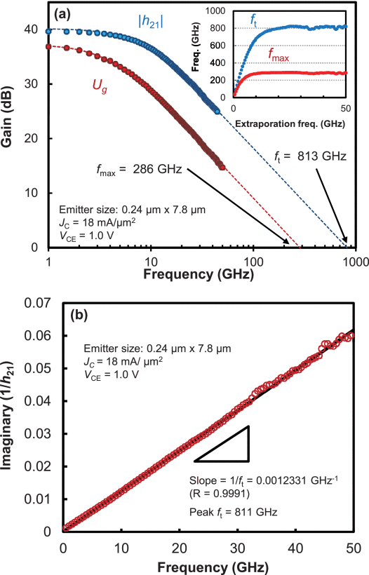
[paper] DHBT with Record ft of 813 GHz

Y. Shiratori, T. Hoshi and H. Matsuzaki,
InGaP/GaAsSb/InGaAsSb/InP Double Heterojunction Bipolar Transistors
With Record ft of 813 GHz
IEEE EDL vol. 41, no. 5, pp. 697-700, May 2020
doi: 10.1109/LED.2020.2982497

Abstract - We fabricated InGaP/GaAsSb/InGaAsSb/InP double heterojunction bipolar transistors (DHBTs) with an aggressive lateral and vertical scaling technology to improve the current gain cutoff frequency (fT) further. A 13-nm-thick GaAsSb/InGaAsSb base and a 40-nm-thick InP collector are used to reduce electron transit time. In addition, the width of the base electrode on each side of the emitter is reduced to about 0.05µm to suppress increases in parasitic collector capacitance. A fabricated DHBT with the emitter size of 0.24µm×7.8 µm exhibits maximum differential current gain of ∼95 and collector-emitter breakdown voltage of 2.6V. At a collector current density of 18 mA/µm2, the DHBT exhibits fT of 813 GHz, which is the highest among all types of transistors measured at a room temperature.
Fig: (a) Current gain ( |h21| ) and Mason’s unilateral power gain (Ug ) of the DHBT as a function of frequency. JC and VCE are 18 mA/μm2 and 1.0 V, respectively. ft and fmax are extrapolated by single-pole fitting. Inset: frequency dependence of extrapolating ft and fmax . (b) Gummel’s ft extraction (imaginary part of 1/h21 as a function of frequency). The red circles and black line show experimental data and a linear fitting, respectively.

URL: https://ieeexplore.ieee.org/stamp/stamp.jsp?tp=&arnumber=9044299&isnumber=9079222