Jun 30, 2020

[paper] Compact Model for SIS Josephson Junctions

A Compact Model for Superconductor-Insulator-Superconductor (SIS) Josephson Junctions
Shamiul Alam, Mohammad Adnan Jahangir and Ahmedullah Aziz, Member, IEEE
Department of Electrical Engineering and Computer Science
University of Tennessee, Knoxville, TN, USA
in IEEE Electron Device Letters, 
DOI: 10.1109/LED.2020.3002448

Abstract: We present a Verilog-A based compact model for the superconductor-insulator-superconductor (SIS) Josephson junction. The model can generate both hysteretic and non-hysteretic current-voltage (I-V) response for the SIS junctions utilizing the Stewart-McCumber damping parameter. We calibrate our model with different SIS samples and demonstrate accurate matching between the simulated and experimental results. We implement temperature effect on the energy gap and the critical current of the superconductor to explore the dynamic trends in device characteristics. We calculate the junction inductance and stored energy as functions of junction current and temperature. We simulate the read/write operations of an SIS junction based cryogenic memory cell to illustrate the usability of our model.
Fig: (a) Device structure of an SIS Josephson junction
(b) the RCSJ model of a Josephson junction.


[paper] 3D Vertical JL GAA Si Nanowire Transistors

Chhandak Mukherjee1, Guilhem Larrieu2 and Cristell Maneuxsup1

Compact Modeling of 3D Vertical Junctionless Gate-all-around Silicon Nanowire Transistors

EuroSOI-ULIS 2020, Sep 2020, Caen (F)

1IMS Laboratory, University of Bordeaux, France

2LAAS-CNRS, Université de Toulouse, France 

HAL: hal.archives-ouvertes.fr/hal-02869216


Abstract: This paper presents a physics based, computationally efficient compact modeling approach for 3D vertical gate-all-around junctionless nanowire transistor (JLNT) arrays designed for future high performance computational logic circuit. The model features an explicit continuous analytical form adapted for a 14 nm channel JLNT technology and has been validated against extensive characterization results on a wide range of JLNT geometry, depicting good accuracy. Finally, preliminary logic circuit simulations have been performed for benchmarking performances of transistor logic circuits, such as inverters and ring oscillators, designed using the developed model.

Fig: The vertical JLNT: (a) SEM image of nanowire arrays, 

(b) single nanowire showing its (c) gate formation 


Acknowledgement: This work is supported by ANR under Grant ANR-18- CE24-0005-01

[webinar] Differentiated FDSOI for mmWave Solutions

WEBEX by IEEE EDS Santa Clara Valley/San Francisco Chapter

Differentiated Fully Depleted SOI (FDSOI) Technology 
for Highly Efficient and Integrated mmWave Wireless Connectivity Solution
Speaker: Dr. Anirban Bandyopadhyay,  Director, Strategic Marketing and Business Analytics, GLOBALFOUNDRIES, Inc., Santa Clara, CA
Friday, July 24, 2020 at 12PM – 1PM PDT

Abstract: The emergence of enhanced mobile broadband (eMBB) connectivity based on mmWave 5G and the emerging prospect of broadband internet to using non-terrestrial mmwave backhaul using low earth orbit (LEO) satellite generated huge interest in the entire telecommunication ecosystem. While mmwave allows huge bandwidth of channels to enable enhanced broadband, it also poses a lot of technical challenges in terms of coverage, generating enough transmitted power efficiently particularly in the uplink, system cost & scaling and long term reliability of the hardware system particularly for infrastructure including Satellite born systems. Current talk will focus on how Silicon technologies based on differentiated fully depleted SOI (FDSOI) can address the above challenges by enabling a highly efficient and integrated radio without compromising on the mmWave performance and reliability. Talk will highlight the technology Figures of Merits (FOMs) for a mmwave phased array system and how a differentiated FDSOI technology platform compares with other silicon technologies in terms of devices and circuits.

Speaker Bio: Dr. Anirban Bandyopadhyay is the Director, Strategic Marketing and Business Analytics within the Mobility & Wireless Infrastructure Business Unit of GLOBALFOUNDRIES, USA. His work is currently focused on hardware architecture & technology evaluations for emerging RF and mmWave applications. Prior to joining GLOBALFOUNDRIES, he was with IBM Microelectronics, New York and with Intel, California where he worked on different areas like RF Design Enablement, Silicon Photonics, signal integrity in RF & Mixed signal SOC’s. Dr. Bandyopadhyay did his PhD in Electrical Engineering from Tata Institute of Fundamental Research, India and Post-Doctoral research at Nortel, Canada and at Oregon State University, USA. He represents Global Foundries in different industry consortia on RF/mmWave applications and is a Distinguished Lecturer of IEEE Electron Devices Society.

More information at the IEEE EDS Santa Clara Valley-San Francisco Chapter Home Page

Subscribe or Invite your friends to sign up for our mailing list and get to hear about exciting electron-device relevant talks. We promise no spam and try to minimize email. You can unsubscribe easily.

Jun 29, 2020

IEEE SSCS-EDS Distinguished Talks (Webinar) Systematic Design of Analog CMOS Circuits Dr. Paul Jespers, UCLouvain, Louvain-la-Neuve, Belgium July 09th, 13h30 (Brasilia Time, GMT-3) https://t.co/d3HL96l2xT https://t.co/FQOFMq4FJG #paper https://t.co/zelqSxMxGI


from Twitter https://twitter.com/wladek60

June 29, 2020 at 11:04AM
via IFTTT

Jun 26, 2020

Creating A Custom ASIC With The First Open Source PDK: The FOSSi foundation now reports on a new, open PDK project launched by Google and SkyWater Technology https://t.co/6G78tYz4c1 #model https://t.co/NOCZS6YMr5


from Twitter https://twitter.com/wladek60

June 26, 2020 at 02:14PM
via IFTTT

Jun 25, 2020

Neurotransistor MatLab Code

Eunhye Baek, Nikhil Ranjan Das, Carlo Vittorio Cannistraci, Taiuk Rim, Gilbert Santiago Cañón Bermúdez, Khrystyna Nych, Hyeonsu Cho, Kihyun Kim, Chang-Ki Baek, Denys Makarov, Ronald Tetzlaff, Leon Chua, Larysa Baraban and Gianaurelio Cuniberti
Intrinsic plasticity of silicon nanowire neurotransistors for dynamic memory and learning functions
Nat Electron (2020). 
DOI: 10.1038/s41928-020-0412-1

Abstract: Neuromorphic architectures merge learning and memory functions within a single unit cell and in a neuron-like fashion. Research in the field has been mainly focused on the plasticity of artificial synapses. However, the intrinsic plasticity of the neuronal membrane is also important in the implementation of neuromorphic information processing. Here we report a neurotransistor made from a silicon nanowire transistor coated by an ion-doped sol–gel silicate film that can emulate the intrinsic plasticity of the neuronal membrane. The neurotransistors are manufactured using a conventional complementary metal–oxide–semiconductor process on an 8-inch (200 mm) silicon-on-insulator wafer. Mobile ions allow the film to act as a pseudo-gate that generates memory and allows the neurotransistor to display plasticity. We show that multiple pulsed input signals of the neurotransistor are non-linearly processed by sigmoidal transformation into the output current, which resembles the functioning of a neuronal membrane. The output response is governed by the input signal history, which is stored as ionic states within the silicate film, and thereby provides the neurotransistor with learning capabilities.

FIG: Illustration of the structural similarity between the ion migration in the neurotransistor (left) and the membrane of a neuron cell in which the ionic current was modulated by a membrane potential (Vmemb) change in the case of the action potential (right)

Code availability: The MatLab code that supports the mathematical model in this article is available
at https://github.com/eunhye8747/MatLab-Code-Neurotransistor

Acknowledgements: This research was supported by the German Excellence Initiative via the Cluster of Excellence EXC1056 Center for Advancing Electronics Dresden (CfAED) and the MSIP (Ministry of Science, ICT and Future Planning), Korea, under the ICT Consilience Creative Program (IITP-R0346-16-1007) supervised by the IITP (Institute for Information & communications Technology Promotion). We acknowledge support from the Initiative and Networking Fund of the Helmholtz Association of German Research Centers through the International Helmholtz Research School for Nanoelectronic Networks (IHRS NANONET) (no. VH‐KO‐606) and German Research Foundation (DFG) via grants MA 5144/9-1, MA 5144/13-1 and MA 5144/14-1; BA4986/7−1, BA4986/8−1. Finally, we thank the INSA-DFG Bilateral Exchange Programme for financial support (IA/ DFG/2018/138, 12 April 2018). The authors thank S. Oswald (IFW Dresden) for the X-ray photoemission spectroscopy analysis of the ion-doped hybrid silicate films and M. Park (NamLab, Dresden) for the insightful discussion about the ionic polarization in the film. We thank R. Nigmetzianov (TU Dresden) for the film analysis.

[paper] Ge Twin-Transistor NVM with FinFET Structure

Siao-Cheng Yan, Chong-Jhe Sun, Meng-Ju Tsai (Student Member, Ieee), Lun-Chun Chen,
Mu-Shih Yeh (Member, IEEE), Chien-Chang Li, Yao-Jen Lee and Yung-Chun Wu (Member, IEEE)
Germanium Twin-Transistor Nonvolatile Memory with FinFET Structure
IEEE J-EDS vol. 8, pp. 589-593, 2020
DOI: 10.1109/JEDS.2020.2999616

Abstract: Germanium is a promising alternative material for use in advanced technology nodes because it exhibits symmetrical mobility of holes and electrons. Embedded nonvolatile memory (NVM) is essential in electronic devices with integrated circuit (IC) technology, including future Ge-based technology. In this paper, we demonstrate Ge twin-transistor NVM with a fin field-effect transistor (FinFET) structure. This Ge twin-transistor NVM exhibits high programming and erasing speeds and satisfactory reliability. Moreover, the masks and fabrication process of this Ge twin-transistor NVM are identical to those of Ge-channel FinFETs. Thus, Ge twin-transistor NVM is a promising candidate for embedded NVM applications in future high-performance Ge complementary metal–oxide–semiconductor technology (CMOS).
FIG:  (a) Schematic top view of the Ge Twin NVM with one fin,
and (b) process flow of the Ge Twin NVM

Acknowledgements: This work was supported in part by Ministry of Science and Technology, Taiwan, under contract MOST 108-2221-E-007-003, and in part by Taiwan Semiconductor Research Institute, Taiwan.


[paper] Statistical modelling of oTFT

Faris, T. M. and Winscom, C. J. 
Statistical modelling of organic thin film transistor behaviour
Organic Electronics (2020, 105846
DOI:10.1016/j.orgel.2020.105846 

Abstract: Three analyses of the expressions describing the electrical characteristics of organic thin film transistors (OTFT's) are presented. The first is the field-independent approach to mobility originally used for inorganic semiconductor materials, often referred to as the Square Law (SQL). The second is appropriate for both the Multiple Trapping and Release (MTR) and the Variable Range Hopping (VRH) descriptions of mobility, where dependence on a transverse field is consistent with the Universal Mobility Law (UML). The third is appropriate for the Extended Gaussian Disorder (EGD) description where an exponential dependence of mobility on the transverse field occurs. In each case master equations have been derived, including Schottky contact effects, where the polarity of the voltage drop across the source and drain contacts is correctly taken into account for the first time. The effect of the bulk semiconductor material beyond the accumulation layer is also accounted for, and defines the sub-threshold performance in a low-voltage regime. A new statistical modelling procedure has been developed to extract the key parameters of these expressions simultaneously from experimental data. For the analysis of TRANSFER data, no more than five parameters are used in the SQL, UML and EGD treatments. All three models are considered so that the effect the choice of model has on the extracted parameters can be revealed; analysis of data from different metallophthalocyanines is used to illustrate the different effects. When the contact resistances correctly take into account possible Schottky-like behaviour, all three descriptions provide equally excellent fits to the data from TRANSFER experiments.  In a following report, a family of copper phthalocyanine-related semi-conductors will be examined in detail using these new analysis procedures to explore the effect of non-peripheral substituent bulk, and aza-nitrogen replacement by CH, on mobility.
Fig: Comparison of Ohmic-only vs. Ohmic+Schottky contact resistance extractions for
the linear region of GdPc2 TRANSFER data for VD=-5V

Acknowledgements: A. K. Ray (Brunel University, Uxbridge) and A. K. Sharma (USAF Research Laboratory) are gratefully acknowledged for providing some resources and experimental data. DZP Technologies Ltd., UK and USAF Research Laboratory, Space Vehicles Directorate, USA are thanked for sponsoring the project, and providing support to TMF.

Jun 24, 2020

[paper] Hot Carrier Degradation in n-MOSFETs

S. Mahapatra and U. Sharma, 
Department of Electrical Engineering,
IIT Bombay, Mumbai 400076, India
A Review of Hot Carrier Degradation in n-Channel MOSFETs
Part I: Physical Mechanism
IEEE TED, vol. 67, no. 7, pp. 2660-2671, July 2020
DOI: 10.1109/TED.2020.2994302

Abstract: Transistor parametric drift due to conduction mode hot carrier degradation (HCD) in n-MOSFETs is reviewed, for long- and short-channel length (LCH) devices having different source/drain (S/D) junction structures. The HCD magnitude and time kinetics shape are discussed for stress under different gate (VG) and drain (VD) biases with varying VG/VD ratio, and without and with substrate bias (VB). Post-dc stress kinetics is discussed. The published data are qualitatively analyzed to identify the roles of different underlying physical mechanisms. In part II of this article, impacts of technology scaling and stress temperature (T) and comparison of dc and ac stress are discussed.
Fig: (a) Schematic of an LDD MOSFET. Carrier heating process, primary and secondary impact ionization, respectively, at VB=0V and VB < 0V, and gate injection are shown. Charges due to HCD in the channel (square), gate–drain overlap (triangle), and spacer (diamond) regions are shown. (b) Energy band diagram showing the energy thresholds for impact ionization, and electron and hole injection over their respective channel-oxide barriers. AHI process is illustrated at (VG–VD) > 0V.


EEE SSCS-EDS Distinguished Talks (Webinar) Low-power Circuits for IoT Dr. Jorge Fernandes, INESC-ID, Lisbon, Portugal. Next Thursday, June 25th, 2:00 PM (Brasilia Time, GMT-3) https://t.co/wJuF6ryZHW #paper https://t.co/6jrZWrKTAh


from Twitter https://twitter.com/wladek60

June 24, 2020 at 02:30PM
via IFTTT

[paper] AlGaN/AlN/GaN/AlGaN photodetector

Khaouani, M., Hamdoune, A., Bencherif, H., Kourdi, Z. and Dehimi, L. 
An ultra-sensitive AlGaN/AlN/GaN/AlGaN photodetector:
Proposal and investigation
Optik (2020). , 217, 164797
DOI:10.1016/j.ijleo.2020.164797 

Abstract: In this paper, an AlGaN/AlN/GaN/AlGaN photodetector high electron mobility transistor is designed and simulated. The proposed structure incorporates an AlN spacer layer between the AlGaN and GaN layers to ensure good control of the two-dimensional gas, which improve, in turn, the device controllability. Besides, an overall figures of merit assessment is performed to highlights the design benefits. The suggested device provides a very high responsivity of 0.2641 A/W, a photocurrent of 1.1 × 10⁻⁷ A, a suitable (Iilumination/Idark) rejection of 10.8, and a high efficiency η of about 77%. The photo and dark current is at 2 V, 87 mA and 8 mA, respectively. A subthreshold slope (SS) of 53 mV/V and 42 mV/V, and a transconductance gm of 260 ms/mm and 180 ms/mm are obtained. The proposed photodetector springly outperforms the HEMT PD designs previously proposed in the literature.
Fig: 2D-structure of AlGaN/AlN/GaN/AlGaN Photodetector HEMT

Acknowledgements: This work was supported by DGRSDT of Ministry of Higher education of Algeria. The work was done in the unit of research of materials and renewable energies (URMER).

[paper] Compact Modeling of Parasitic FET capacitance

Sharma, S. M., Singh, A., Dasgupta, S., & Kartikeyan, M. V. 
A review on the compact modeling of parasitic capacitance: 
from basic to advanced FETs. 
Journal of Computational Electronics
DOI: 10.1007/s10825-020-01515-4

Abstract: This paper presents a review on the development of parasitic-capacitance modeling for metal–oxide–semiconductor feldefect transistors (MOSFETs), covering models developed for the simple parallel-plate capacitance and the nonplanar and coplanar plate capacitances required for the intrinsic and extrinsic part of such devices. A comparative study of various extrinsic capacitance models with respect to a reference model is used to analyze the benefts of the various approaches. Capacitance models for basic MOSFETs and advance multigate FETs with two-dimensional (2D) and three-dimensional (3D) structures are reviewed. It is found that the elliptical feld lines between the gate electrodes and source/drain region are modeled very well, while deviations of ±2% in the orthogonal plate capacitance are observed when the gate electrode thickness is varied from 5 to 20nm.
Fig: The 3D structure of a FinFET

Acknowledgements: The authors would like to thank the Department of Electronics and Communication Engineering, IIT Roorkee, for their valuable support in carrying out this research work.


[paper] SPICE Model for Bipolar Resistive Switching Devices

Miranda, Enrique, and Jordi Suñé
Departament d’Enginyeria Electrònica,
UAB, 08193 Barcelona, Spain
Fundamentals and SPICE Implementation of the Dynamic Memdiode Model
for Bipolar Resistive Switching Devices
(2020 - techrxiv.org)

Abstract: This paper reports the fundamentals and SPICE  implementation of the dynamic memdiode model (DMM) for the  conduction characteristics of bipolar resistive switching (RS)  devices. Following Chua’s memristive devices theory, the  memdiode model comprises two equations, one for the electron  transport based on a heuristic extension of the quantum pointcontact model for filamentary conduction in dielectrics and a  second equation for the internal memory effect related to the  reversible displacement of atomic species within the oxide film.  The DMM represents a breakthrough with respect to the previous  quasi-static memdiode model (QMM) since it describes the  memory state of the device as a rate balance equation  incorporating both the snapback and snapforward effects,  features of utmost importance for the accurate and realistic  simulation of the RS phenomenon. The DMM allows simple setting  of the memory state initial condition as well as separate modeling  of the set and reset transitions. The model equations are  implemented in the LTSpice simulator using an equivalent  circuital approach with behavioral components and sources. The  practical details of the model implementation and its use are  thoroughly discussed.   
Fig: Hysteretic behavior of the filamentary-type I-V characteristic.
Filament stages: A) formation, high resistance state (HRS), B) completion, C) expansion,
D,F) complete expansion, low resistance state (LRS), G) dissolution, I) rupture.

Supplementary information: The memdiode model script for LTSpice XVII reported in this Appendix includes not only the DMM but also the QMM. It is important to activate one of the options at a time (DMM or QMM) by inserting asterisks (*) in the corresponding lines. The parameter list, I-V, and Auxiliary functions sections are common to both approaches. This does not mean that the obtained curves will be identical. The meaning of the parameters is discussed in the text and in previous papers.

LTSPICE script
.subckt memdiode + - H
*created by E.Miranda & J.Suñé, June 2020
.params
+ H0=0 ri=50
+ etas=50 vs=1.4
+ etar=100 vr=-0.4
+ imax=1E-2 amax=2 rsmax=10
+ imin=1E-7 amin=2 rsmin=10
+ vt=0.4 isb=200E-6 gam=1 gam0=0 ;isb=1/gam=0 no SB/SF
+ CH0=1E-3 RPP=1E10 I00=1E-10
*Dynamic model
BV A 0 V=if(V(+,-)>=0,1,0)
RH H A R=if(V(+,-)>=0,TS(V(C,-)),TR(V(C,-)))
CH H 0 1 ic={H0}
*Quasi-static model
*BH 0 H I=min(R(V(C,-)),max(S(V(C,-)),V(H))) Rpar=1
*CH H 0 {CH0} ic={H0}
*I-V
RE + C {ri}
RS C B R=RS(V(H))
BD B - I=I0(V(H))*sinh(A(V(H))*V(B,-))+I00
RB + - {RPP}
*Auxiliary functions
.func I0(x)=imin+(imax-imin)*limit(0,1,x)
.func A(x)=amin+(amax-amin)*limit(0,1,x)
.func RS(x)=rsmin+(rsmax-rsmin)*limit(0,1,x)
.func VSB(x)=if(x>isb,vt,vs)
.func ISF(x)=if(gam==0,1,pow(limit(0,1,x),gam)-gam0)
.func TS(x)=exp(-etas*(x-VSB(I(BD))))
.func TR(x)= exp(etar*ISF(V(H))*(x-vr))
.func S(x)=1/(1+exp(-etas*(x-VSB(I(BD)))))
.func R(x)=1/(1+exp(-etar*ISF(V(H))*(x-vr)))
.ends

Acknowledgements: This work was funded by the WAKeMeUP 783176 project, co‐ funded by grants from the Spanish Ministerio de Ciencia, Innovación y Universidades (PCI2018‐093107 grant) and the ECSEL EU Joint Undertaking and by project TEC2017-84321- C4-4-R funded by the Spanish Ministerio de Ciencia, Innovación y Universidades. Dr. G. Patterson and Dr. A. Rodriguez are greatly acknowledged for their contributions to the development of the ideas reported in this work


Jun 23, 2020

Webinar Series by Distinguished Experts

 
 The National Academy of Sciences, India (NASI)
- Delhi Chapter-
and
 
 MHRD-Institution Innovation Council (IIC)
Deen Dayal Upadhyaya College Chapter
(University of Delhi)
Under the aegis of DBT Star College Program
 
Jointly Organizes
Webinar Series by Distinguished Experts
 June 25, 2020 @ 10 am Indian Standard Time
Printed and Flexible Electronics and Devices
Dr. Jin-Woo Han
Research Scientist, Center for Nanotechnology,
NASA Ames Research Center, Moffett Field, California, USA
 
July 03, 2020 @ 04:30 pm Indian Standard Time
New chemistry and physics in magnetic oxides
Prof. J. Paul Attfield, FRS FRSE FRSC, Foreign Fellow INSA
Professor of Materials Science at Extreme Conditions
School of Chemistry, Centre for Science at Extreme Conditions,
The University of Edinburgh, Edinburgh
 July 09, 2020 @ 06:30 pm Indian Standard Time
Prof. Katepalli Sreenivasan, Foreign Fellow INSA
Dean Emeritus of NYU Tandon School of Engineering;
The Eugene Kleiner Professor for Innovation in Mechanical Engineering;
Professor of Physics (Faculty of Arts and Science);
Mathematics (Courant Institute of Mathematical Sciences)
 

July 10, 2020 @ 01:30 India Standard Time
Can Future Energy Needs be met Sustainably?
Prof. Sir Chris Llewellyn Smith, FRS, FAPS (USA), Honorary Fellow, IOP (UK), Foreign Fellow INSA(India)
Rudolf Peierls Centre for Theoretical Physics
Parks Road, Oxford OX1 3PU
 July 11, 2020 @ 03:30 pm Indian Standard Time
Are we there yet? How do cells find their way?
Prof. Philip K. Maini, FRS, FIMA, FRSB, FMedSci, Foreign Fellow INSA (India)
Wolfson Centre for Mathematical Biology
Mathematical Institute, Andrew Wiles Building, Radcliffe Observatory Quarter
Woodstock Road, Oxford
 July 14, 2020 @ 04:30 pm Indian Standard Time
The influence of infection on Society before Covid19
Prof. Sir Peter Julius Lachmann, FRS, FRCP, FRCPath, FMedSci, Foreign Fellow INSA(India)
Fellow, Emeritus Sheila Joan Smith Professor of Immunology
Christ College, University of Cambridge
No registration fee to attend the Lecture. However, all interested should register via Google form on or before June 22, 2020 to attend the lectures via CISCO Webex/Google Meet. Link for Google form:

Organizer: Prof. Ajoy Ghatak, Chairperson - NASI Delhi Chapter & Prof. Anurag Sharma, Secretary - NASI Delhi Chapter
Coordinator:
Dr. Manoj Saxena, MNASc and Executive Committee Member-NASI Delhi Chapter
Associate Professor, Deptt. of Electronics, Deen Dayal Upadhyaya College, University of Delhi, New Delhi
Dr. Geetika Jain Saxena, Associate Professor, Department of Electronics, Maharaja Agrasen College, University of Delhi, New Delhi

Stay up to date with the latest developments in the MEMS areas with IEEE RightNow. Access for J-MEMS. Enjoy temporary Open Access to selected featured publications https://t.co/mxoRhbT802 #paper https://t.co/9h5EV2mEBf


from Twitter https://twitter.com/wladek60

June 23, 2020 at 11:56AM
via IFTTT

Jun 22, 2020

[paper] “Extrinsic” Compact Model of the MOSFET Drain Current

V. O. Turin, R. S. Shkarlat, G. I. Zebrev, B. Iñiguez and M. S. Shur
The “Extrinsic” Compact Model of the MOSFET Drain Current Based on a New Interpolation Expression for the Transition Between Linear and Saturation Regimes with a Monotonic Decrease of the Differential Conductance to a Nonzero Value
2020 4th IEEE EDTM, Penang, Malaysia
2020, pp. 1-4
doi: 10.1109/EDTM47692.2020.9117810

Abstract: Previously, we proposed a new interpolation expression to bridge the transition between the linear and the saturation regimes of “intrinsic” MOSFET. This approach, in contrast to the traditional one, gives a monotonic decrease of the differential conductance from the maximum value in the linear regime to the minimum value in the saturation regime. Later, we proposed a linear approximation for an “extrinsic” MOSFET drain current dependence on the “extrinsic” drain bias in the saturation regime for not very high drain bias when nonlinear effects can be neglected. To obtain this approximation, an equation for the output differential resistance of the “extrinsic” MOSFET in saturation regime was obtained, that is similar to the result known from the theory of the common source MOSFET amplifier with source degeneration. In this paper, we combine these two results and present an “extrinsic” compact model for a short-channel MOSFET above threshold drain current with proper account of the differential conductance in the saturation regime.


[paper] Analog/RF Tri-metal Gate FinFET

N. G. P, S. Routray and K. P. Pradhan
Assessment of Analog/RF performances for 10 nm Tri-metal Gate FinFET
2020 4th IEEE EDTM; 2020, pp. 1-4
Penang, Malaysia
DOI: 10.1109/EDTM47692.2020.9117846

Abstract: Reduction in parasitic capacitance and resistance in FinFET is quite necessary in order to achieve high performance. In this paper, an intensive study on structural advancement in three different ways is implemented in basic FinFET structure such as (a) addition of thin silicide layer as interfacial layer between the contact and source/drain (b) extended and elevated source/drain (c) addition of hybrid spacer. Additionally, comparative study on the analog and RF performance is performed and analyzed for this structure between single material gate (SMG) and tri material gate (TMG) FinFET with all above enhancements. The analog parameters that have been analyzed are transconductance (gm), transconductance generation factor (TGF), output conductance (gd), and intrinsic gain (gm/gd). Similarly, the RF parameters like gate capacitance (CGG), cut-off frequency (fT), transconductance frequency product (TFP), gain frequency product (GFP), and gain transconductance frequency product (GTFP) are reported. Even though there is a degradation in the mobility for the TMG FinFET, but on a whole provides better performance. Furthermore, the effect of temperature on the drain current and transconductance has been shown for the TMG structure by varying the temperature from 200 to 350K with intervals of 50K which would be the extension to this paper. Analysis gives a potential overview on different structural improvement in order to achieve higher performance.
Fig. I. Top view of the proposed FinFET structure

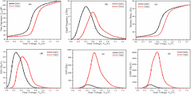
Fig. II. (a) Gate capacitance (b) cutoff frequency (c) intrinsic delay (d) TFP (e) GFP (f) GTFP plots by variation of gate material.


[virtual] ToM2020/2 Announcement

ToM2020/2 Course
September, 8th, 2020
    14.00-17.30    Danilo Gerna (Melexis Technologies), “Advanced Hall Element Based Magnetic Sensors Front End Design”

September, 9th, 2020
    9.00-12.30    Carlo Samori (Milan Politechnic), “PLL: From Analog to Digital and Recent Trends”
    14.00-17.30    Alex Tranca (Infineon), “Robust Design of Smart Power ICs for Automotive Applications, with Focus on Load Current Sensing”

September, 10th, 2020
    9.00-12.30    Alfio Dario Grasso (Univ. Catania), “Ultra-Low Power Amplifiers for IoT Nodes”
    14.00-17.30    Gabriella Ghidini (STMicroelectronics), “Dielectric Reliability in Microelectronics”

In this particular situation, the PhD School at University of Milan-Bicocca decided to fully support the costs of the ToM2020/2 course, whose participation will then be free-of-charge for the attendees. However, for proper managing internet access to the virtual ToM2020/2 course, registration is mandatory at the following website:
http://www.innotechevents.com/index.php?page=ToM/RegistrationForm.html

Only registered participants will receive access information for the course.
At the end of the course, an exam will be proposed for certifying the positive attendance (please register to the exam with the course registration).
We look forward to virtually meeting you !!!!

More information at:
http://www.innotechevents.com/index.php?page=ToM/ToM.html

[virtual] IEEE EDS DL Mini-Colloquium at MIXDES Wroclaw


EDS Distinguished Lecturer Mini-Colloquium 
"Semiconductor-based sensors - technology, modeling, applications" 
(virtual at MIXDES), June 27, 2020
Chairs: Wladek Grabinski, Daniel Tomaszewski

10.00-10.45
Arokia Nathan "Ultralow Power, High-Resolution Sensor Interfaces"
EDS Distinguished Lecturer, Cambridge Touch Technologies, UK; E-mail: an299@cam.ac.uk
10.45-11.30
Mike Schwarz "Sensor Design – From Prototype to Series"
Robert Bosch GmbH, 72703 Reutlingen,Germany; E-mail: Mike.Schwarz@de.bosch.com
12.00-12.45
Benjamin Iñíguez "Compact Modeling and Parameter Extraction for Oxide and Organic Thin Film Transistors (TFTs) from 150K to 350K"
EDS Distinguished Lecturer, Department of Electrical, Electronics Engineering and Automatic Control Engineering, Universitat Rovira i Virgili, 43007 Tarragona, Spain; E-mail: benjamin.iniguez@urv.cat
12.45-13.30
Teoder Gotszalk " Microsystem Electronics and Photonics "
Faculty of Microsystem Electronics and Photonics, Wroclaw University of Technology, Poland; E-mail: teodor.gotszalk@pwr.edu.pl
13.30-14.15
Mina Rais-Zadeh "Phase change electro-optical devices for space applications" (recorded)
EDS Distinguished Lecturer, NASA Jet Propulsion Lab., California Institute of Techn., USA; E-mail: minar@umich.edu

Jun 19, 2020

Jun 18, 2020

[Short Course] Modeling and Simulation of Nano-Transistors

Short Course
Modeling and Simulation of Nano-Transistors
6 - 10 July 2020 at Outreach Auditorium,IIT Kanpur
http://www.iitk.ac.in/nanolab/sc2020/
by Prof. Yogesh S. Chauhan
Nanolab, IIT Kanpur
http://home.iitk.ac.in/~chauhan/

Aim: VLSI design will soon use transistors whose size will be as small as 10nm. The aim of this short course is to educate and train bright minds on different aspects of Nano-transistors. Modeling especially compact modeling is the heart of circuit simulation. TCAD simulations are used for early device design and to understand the internal physics of transistor. Electrical characterization includes current and capacitance voltage measurement of transistor. RF measurement is an exciting area which involves understanding of devices as well as high frequency effects. This short course will cover various topics in modeling, simulation and characterization of transistors especially at nanoscale.

Topics: (1) VLSI design and Nanoelectronics, (2) Physics and Operation of MOSFET, (3) SPICE and Circuit simulation, (4) TCAD simulation: Theory and demonstration, (5) Compact Modeling: Theory and demonstration, (6) Scaling and Moore's Law, (7) Nano-Transistors: FinFET, FDSOI, Negative Capacitance FET, Nanosheet FETs, 2D-FETs etc. (8) Characterization: Current and capacitance measurement, (9) RF CMOS and GaN High Electron Mobility Transistors

Hands-on Sessions: (1) Verilog-A coding, (2) SPICE ckt. Simulation, (3) TCAD Simulation, (4) Parameter Extraction

Coordinator: Prof. Yogesh S. Chauhan Dept. of Electrical Engg., IIT Kanpur

Registration: This short course has been postponed to end of this year or early next year due to ongoing pandemic. New Dates will be announced once normalcy returns in the country.

Jun 17, 2020

A Benchmark Study Of Complementary-Field Effect Transistor (#FET) Process Integration Options: Comparing #Bulk vs. #SOI vs. DSOI Starting Substrates https://t.co/rYE24rym7L #paper https://t.co/T3ECdVJa5c


from Twitter https://twitter.com/wladek60

June 17, 2020 at 05:02PM
via IFTTT

[paper] CV of Graphene–Silicon Heterojunction Photodiodes

Sarah Riazimehr,  Melkamu Belete,  Satender Kataria,  Olof Engström and Max Christian Lemme
Capacitance–Voltage (C –V) Characterization 
of Graphene–Silicon Heterojunction Photodiodes
Advanced Optical Materials 
First Published Open Access: 07 May 2020
DOI: 10.1002/adom.202000169

Abstract: Heterostructures of 2D and 3D materials form efficient devices for utilizing the properties of both classes of materials. Graphene/silicon (G/Si) Schottky diodes have been studied extensively with respect to their optoelectronic properties. Here, a method to analyze measured capacitance–voltage (C –V) data of G/Si Schottky diodes connected in parallel with G/silicon dioxide/Si (GIS) capacitors is introduced. The accurate extraction of the built‐in potential (Φbi) and the Schottky barrier height (SBH) from the measurement data independent of the Richardson constant is also demonstrated.
Figure 2
Fig.: a) Cross section of the test device showing both MIS and GIS regions. b) Small‐signal C –V characteristics of Dtest (line) compared to a theoretically calculated C –V curve (dashed ) at 10 kHz.

Acknowledgements: Financial support from the European Commission (Graphene Flagship, 785219, 881603) and the German Ministry of Education and Research, BMBF (GIMMIK, 03XP0210) is gratefully acknowledged.

[paper] Compact Model for Ferroelectric FET

Lu, Darsen, Sourav De, Mohammad Aftab Baig, Bo-Han Qiu, and Yao-Jen Lee
Computationally efficient compact model for ferroelectric field-effect transistors 
to simulate the online training of neural networks
Semiconductor Science and Technology (2020)
DOI: 10.1088/1361-6641/ab9bed

Abstract: In this paper, a compact drain current formulation that is simple and adequately computationally efficient for the simulation of neural network online training was developed for the ferroelectric memory transistor. Tri-gate ferroelectric field effect transistors (FETs) with Hf0.5Zr0.5O2 gate insulators were fabricated with a gate-first high-k metal gate CMOS process. Ferroelectric switching was confirmed with double sweep and pulse programming and erasure measurements. Novel characterization scheme for drain current was proposed with minimal alteration of ferroelectric state in subthreshold for accurate threshold voltage measurements. The resultant threshold voltage exhibited highly linear and symmetric across multilevel states. The proposed compact formulation accurately captured the FET gate-bias dependence by considering the effects of series resistance, Coulomb scattering, and vertical field dependent mobility degradation.
Fig.: Transmission electron micrograph of the fabricated tri-gate Fe
finFET device across the fin, with approximately 60 nm fin width, 30 nm fin
height, and 10 nm HZO Fe layer.

Acknowledgements: This work was jointly supported by the Ministry of Science and Technology (Taiwan) grant MOST–108–2634–F–006–08 and is part of research work by MOST’s AI Biomedical Research Center. We are grateful to the Taiwan Semiconductor Research Institute for nanofabrication facilities and services and to Dr. Wen-Jay Lee and Nan-Yow Chen of the National Center for High-Performance Computing for helpful suggestions on AI computation. This manuscript was edited by Wallace Academic Editing.

Jun 16, 2020

Learning with brain chemistry https://t.co/UJRbFdHuUh #paper https://t.co/PB4Ty0moUg


from Twitter https://twitter.com/wladek60

June 16, 2020 at 05:39PM
via IFTTT

[paper] TFT Compact Modeling

Arun Dev Dhar Dwivedi, Sushil Kumar Jain, Rajeev Dhar Dwivedi and Shubham Dadhich
Numerical Simulation and Compact Modeling 
of Thin Film Transistors for Future Flexible Electronics
Submitted: July 4th 2019Reviewed: October 28th 2019Published: June 10th 2020
DOI: 10.5772/intechopen.90301

Abstract: In this chapter, we present a finite element method (FEM)-based numerical device simulation of low-voltage DNTT-based organic thin film transistor (OTFT) by considering field-dependent mobility model and double-peak Gaussian density of states model. Device simulation model is able to reproduce output characteristics in linear and saturation region and transfer characteristics below and above threshold region. We also demonstrate an approach for compact modeling and compact model parameter extraction of organic thin film transistors (OTFTs) using universal organic TFT (UOTFT) model by comparing the compact modeling results with the experimental results. Results obtained from technology computer-aided design (TCAD) simulation and compact modeling are compared and contrasted with experimental results. Further we present simulations of voltage transfer characteristic (VTC) plot of polymer P-channel thin film transistor (PTFT)-based inverter to assess the compact model against simple logic circuit simulation using SmartSpice and Gateway.
Fig.: Schematic cross-sectional diagram of organic TFTs 
along with the chemical structure of SAM and organic semiconductor.

Acknowledgments: The authors are thankful to SERB, DST, Government of India, for the financial support under Early Career Research Award (ECRA) for Project No. ECR/2017/000179.

#Intel’s #10nm Node: Past, Present, and Future [EETimes] https://t.co/P3Fi3xUogJ #paper https://t.co/QoFX5z22br


from Twitter https://twitter.com/wladek60

June 16, 2020 at 02:31PM
via IFTTT

[slides] (Ultra-) Wide-Bandgap Devices

(Ultra-) Wide-Bandgap Devices: Reshaping the Power Electronics Landscape
Presenter Dr. Yuhao Zhang, Assistant Professor,
Center for Power Electronics Systems, Virginia Tech
IEEE EDS SCV-SF Seminar 
Friday, June 12, 2020 at 12PM – 1PM PDT

Abstract: Power electronics is the application of solid-state electronics for the control and processing of electrical energy. It is used ubiquitously in consumer electronics, electric vehicles, data centers, renewable energy systems, and smart grid. The power semiconductor device, as the cornerstone technology in power electronics, is key to improving the efficiency, cost and form factor of power electronic systems.  Recently, the power electronics landscape has been significantly reshaped with the production and application of power devices based on wide-bandgap (WBG) semiconductors, such as gallium nitride (GaN) and silicon carbide (SiC). Besides advancing the performance of traditional power systems, WBG devices have also enabled many emerging applications that are beyond the realm of silicon (Si) as well as changed the manufacturing paradigm of power electronics. On the horizon is the power devices based on ultra-wide-bandgap (UWBG) materials, which promises superior performance over GaN and SiC and is at the relatively early stage of research development.  This talk will provide a comprehensive overview of major WBG and UWBG power device technologies, spanning materials, devices, reliability and applications. Some research projects in the PI’s group in collaboration with industry will also be introduced.
FIG: WBG Semiconductor: Superior Power Semiconductor Over Si

The seminar presentation is now available on our IEEE EDS SCV-SF webpage:
http://site.ieee.org/scv-eds/files/2020/06/SCV_SF_EDS_Yuhao_Zhang_excerpt.pdf

More information at the IEEE EDS Santa Clara Valley-San Francisco Chapter Home Page. Subscribe or Invite your friends to sign up for our mailing list and get to hear about exciting electron-device relevant talks. We, EDS SCV-SF, promise no spam and try to minimize email. You can (un)subscribe easily.


Jun 15, 2020

[paper] Future of Ultra-Low Power SOTB CMOS

Nobuyuki Sugii1, Shiro Kamohara2, Makoto Ikeda3
The Future of Ultra-Low Power SOTB CMOS Technology and Applications
NANO-CHIPS 2030. The Frontiers Collection. Springer, Cham
DOI: 10.1007/978-3-030-18338-7_6
1.Hitachi, Ltd.Tokyo, Japan
2.Renesas Electronics Corp.Tokyo, Japan
3.The University of Tokyo, Japan

Abstract: Ultra-low power technology has drawn much attention recently as the number of connecting (Internet-of-Things) devices rapidly increases. The silicon-on-thin-buried oxide (SOTB) technology is a CMOS device technology that uses fully depleted silicon-on-insulator (FDSOI) transistors with a thin buried oxide layer enabling enhanced back-bias controllability and that can be monolithically integrated with the conventional bulk CMOS circuits. It can significantly reduce both the operation and the standby powers by taking advantage of low-voltage operation and back-biasing, respectively. In this chapter, advantages of the SOTB technology in terms of ultra-low power, circuits design and chip implementation examples including ultra-low power micro-controllers operating with harvested power, reconfigurable logic circuits, analog circuits, are reviewed, and a future perspective is shown.
Fig.: Schematic cross section of SOTB transistors. Hybrid bulk transistors are shown. SOTB  transistors are used in low-voltage (< ~1.5 V) logic and analog circuits including SRAMs. Bulk  transistors are used in peripheral, ESD-protection, high-voltage analog and power circuits, on-chip,  flash memory, and reuse of legacy circuits

Acknowledgements: The part of the work, especially on developing the SOTB technology by the Low-power Electronics Association and Project (LEAP), is supported by the Ministry of Economy, Trade and Industry (METI) and the New Energy and Industrial Technology Development Organization (NEDO). Part of the chip fabrication by the universities is done under a support of VLSI Design and Education Center (VDEC) in collaboration with Renesas Electronics Corporation, Cadence Corporation, Synopsys Corporation and Mentor Graphics Corporation.

IEEE PS Webinar "G2V and V2G Technologies in Electric Vehicles"

IEEE Photonics Society Student Chapter of Mangalam College of Engineering is geared up with webinar series to provoke the little spark in you

  • Date:16-06-2020
  • Time:10:30 - 11:30 AM IST
  • Pre registration link: https://bit.ly/3dTeDzP
  • Topic: G2V and V2G Technologies in Electric Vehicles
  • Speaker: Dr.Sreejith.S; Assistant Professor,
    Department of Electrical Engineering,
    National Institute of Technology, Silchar, Assam

We, IEEE Photonics Society Student Chapter, invite you all to join this webinar and take away some useful stuffs in this quarentine. Registration free!!! See you there. All registered participants are honoured with e-certificates

Webinar Link: https://bit.ly/2ZgJuBY
For further queries contact our coordinators:
Alsufiyan   : +91 7736598136
Nandhu : +91 9061383258

Stay Safe, Enjoy learning!! Stay updated with us for more exciting events!...