1
Department of Electrical and Electronic Teaching,
College of Information Science and Engineering,
Huaqiao University, Xiamen 361021, China
2
Department of Electronic Engineering, Jinan University, Guangzhou 510632, China
*
Correspondence: yufei_jnu@126.com; Tel.: +86-0592-6162-385
†
These two authors contributed equally to this work.
Received: 10 May 2019 / Accepted: 12 June 2019 / Published: 14 July 2019
Abstract
:
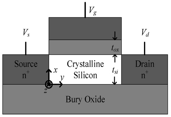
A surface-potential-based analytical I-V model of single-gate (SG) silicon-on-insulator (SOI) MOSFETs in full-depletion (FD) mode is proposed and compared with numerical data and Khandelwal’s experimental results. An explicit calculation scheme of surface potential, processing high computation accuracy and efficiency, is demonstrated according to the derivation of the coupling relation between surface potential and back-channel potential. The maximum absolute error decreases into 10−7 V scale, and computation efficiency is improved substantially compared with numerical iteration. Depending on the surface potential, the drain current is derived in closed-form and validated by Khandelwal’s experimental data. High computation accuracy and efficiency suggest that this analytical I-V model displays great promise for SOI device optimizations and circuit simulations.
Keywords:
silicon-on-insulator MOSFETs; surface potential; back-channel potential; full-depletion; analytical I-V model


No comments:
Post a Comment