Sep 30, 2026

[EUMW.EU] IHP Open Source Toolchain

Open-source Toolchain in RF and Digital Design
08:30 - 12:50; Monday 5 October 2026
European Microwave Week 

The European Chips Act serves as a strategic roadmap to secure technological sovereignty by aiming for a 20% global market share in semiconductors by 2030. The goal is to minimize the geopolitical supply chain risks and foster a self-sufficient ecosystem. Democratization of hardware development through the development of open-source EDA tools is a key pillar in these aspects. This would lower the entry barriers for SMEs and researchers and ultimately accelerate a collaborative and transparent era of European silicon innovation. There are multiple EU funded projects have started from last few years. These projects are set to offer robust process design kits (PDK) for open-source tools. In parallel, existing open-source tools for IC design are being further enhanced to include necessary functionalities for complete design flow for digital, analogue and RF design. Aligning with above mentioned goals, multiple private, academic, and commercial entities have stepped up towards the development. This workshop aims to share a glimpse of activities in open-source EDA tools developments and chip design activities in Europe. It would begin with a talk about current EU projects and the statuses in open-source EDA development. Then there will be two talks about digital and RF design flow using open-source tools. The final talk is about electro-magnetic simulation for RF circuits. Overall, this workshop is targets to publicize the open-source activities towards the building of a collaborative society in chip design domain. 

The event is aimed at IC designers, researchers, PhD candidates and engineers who already have a basic understanding of chip design and EDA workflows. Familiarity with digital, analogue or RF design will help you get the most from the sessions.

This workshop, chaired by the IHP Team: Corrado Carta, Sergei Andreev, and Farabi Ibne Jamal, gives you a practical view on the following Open-Source R&D Topics:
  • European Open-Source EDA projects currently stand
    • Sergei Andreev, IHP
  • How digital design flows can be built with Open-Source tools
    • Frank Kagan Gurkaynak, ETH Zürich
  • How Open-Source tools are being applied to RF design 
    • Harald Pretl, Johannes Kepler Universität Linz
  • How Open-Source EM simulation fits into RF circuit development
    • Giovanni Di Pietrantonio, IHP and Volker Mühlhaus, MCS, GmbH
Join the IHP OpenPDK Team if you want to understand where open-source chip design is heading, what is already usable today, and how these tools could complement your own work. Register at the EuMW website.


Sep 29, 2026

IEEE EDS/SSCS/CAS Mini-Colloquium

Friday 11 September 2026
UIB; Sa Riera Building
C/ de Miquel dels Sants Oliver, 2
07122 Palma

Professors Benjamin Iniguez, URV and Rodrigo Picos, UIB, have organize joint IEEE EDS/SSCS/CAS Mini-Colloquium as an integral part of the recent ESSERC2026 in Palma de Mallorca. All the MQ participants followed the MQ program as follows:

Mini-Colloquium Agenda
9:00 - 09:05 Opening

9:05-9:15 Tribute to Michael S. Shur

9:05-9:15 Tribute to José Epifânio da Franca 

9:15-10:05 Leveraging semiconductor technology for the benefit of society
Fernando Guarin (Director of IEEE Division I)

10:05-10:55 Power efficient WBG devices for the green transition
Mikael Ostling (KTH, SE)

10:55-11:25 Coffee Break

11:25-12:15 Holistic solutions to future computing - not only scaling
Francesca Iacopi (Purdue University, US)

12:15-13:05 Status of the Compact modeling and its Verilog-A standardization
Wladek Grabinski (MOS-AK, CH and IHP OpenPDK, DE)

13:05-14:25 Lunch

14:25-15:15 Graphene thin film technology for neural interfaces
José Antonio Garrido (ICN2, Barcelona, Spain)

15:15-16:05 Energy-Efficient Analog IC Design:
Exploring Solutions at Device, Circuit and System Levels
Antonio López (Public University of Navarra, Spain)

[paper] TCAD Modeling of SB Diode

Pedro Paulo Pessoa Oliveira1,2, Andreas Mai1,3, Norbert Herfurth1, 
and Davies William de Lima Monteiro2
TCAD Modeling of Schottky-Diode in an open-source SiGe BiCMOS technology
In 2026 40th Symposium on Microelectronics Technology and Devices 
SBMicro, pp. 1-4. IEEE, 2026
DOI: 10.1109/SBMicro70495.2026.11684441

1. IHP, Frankfurt (Oder), Germany
2. Department of Electrical Engineering, UFMG - Belo Horizonte-MG, Brazil
3. University of Applied Sciences Wildau, Germany

Abstract: Accurate simulation of Schottky barrier diodes (SBDs) is challenging because standard idealized models fail to capture non-ideal interface physics, such as Fermi-level pinning and image-force lowering. This paper presents an enhanced Technology Computer-Aided Design (TCAD) methodology to model an SBD from the IHP SG13G2 130-nm open-source SiGe BiCMOS technology. To overcome limitations of conventional simulations that often rely on oversimplified assumptions and empirical fitting, this work explicitly incorporates interface en- ergy states into the simulation, specifically modeling the fun- damental pinning mechanisms driven by Metal-Induced Gap States (MIGS). By calibrating the TiSi2/Si interface using the theoretical slope parameter, a value of 0.503 V was determined for the zero-bias barrier height. The resulting physics-based model captures the true rectifying nature of the contact and accurately reproduces the electrical characteristics targeted by the empirical model, achieving a nominal forward voltage drop of 0.39 V and a realistic reverse leakage current of 29.3 nA at -2.5 V. Ultimately, this paper shows the innovation and education gain of open- source foundry data by showcasing an open innovation path for a targeted near-industry device development flow.
FIG: a.) Energy band diagram of the Schottky diode at V=0V. Thecoordinate x = 0 corresponds to the TiSi2/n-Si Schottky interface. The inset displays the 2D device schematic, with the solid black line indicating the multi-segment cut-path used to extract the energy levels across the anode, n-buried layer and n-well RT to cathode contact. b.) Comparison of the simulated DC current-voltage (IV) characteristics between the proposed TCAD model and the standard SPICE macromodel.

Acknowledgment: The authors thank IHP for the open-source PDK and the collaborative research. They also thank Universidade Federal de Minas Gerais (UFMG) and the Brazilian Microelectronics Society (SBMicro) for supporting this work. Finally, gratitude is extended to S. Srivastava and B. Sake for their valuable guidance.

Sep 28, 2026

[NanoIC] Workshop

NanoIC Pilot Line Workshop
Next logic, memory, and chiplet technologies to enable future system innovation
October 1, 2026; Sede Turismo Andaluz; 40 Compañía Str. Málaga, Spain

Workshop Agenda

10:00 - 10:10 Welcome
10:10 - 10:30 Marie Garcia Bardon 
Short Introduction to EU Chips Act NanoIC Pilot Line
10:30 - 11:30 Nicolas Pantano 
Enabling Chiplet Architectures Through Advanced Packaging And High-Density Interconnects
11:30 - 12:00 Coffee break
12:00 - 13:00 Fernando García Redondo 
Opportunities in memory scaling: design-technology co-optimization for SRAM and emerging memories
13:00 - 14:00 Marie Garcia Bardon 
Advanced Logic Scaling: Technologies for the sub-2nm

Free Registration Online Workshop  
               https://u.uma.es/icc/workshop

Sep 26, 2026

[ChipFoundry] December Shuttle: Commitment deadline moved to November 4th

Sep 25, 2026

[paper] EKV compact modeling for oxide CTFTs

Mingyu Zhuang, Zhiyuan Wang, Baochuan Liu, Jiawei Zhang, Qian Xin, Aimin Song
Neural-network-assisted EKV compact modeling for complementary oxide thin-film transistors
Appl. Phys. Lett. 129, 123504 (2026)
DOI: 10.1063/5.0349365

1. Shandong Technology Center of Nanodevices and Integration, Uni. Shandong (CN)
2. Department of Electrical and Electronic Engineering, Uni. Manchester (UK)
3. Southern University of Science and Technology, Shenzhen (CN)

ABSTRACT: This work reports a neural-network-assisted Enz–Krummenacher–Vittoz (EKV) compact-modeling framework for complementary oxidethin-film transistors (TFTs). The neural network is used as a bias-dependent effective-parameter generator for the equivalent mobility and onset voltage, while the drain current is calculated by the analytical EKV current core. This strategy represents defect-, contact-, and bias-dependent nonidealities of oxide TFTs through effective quantities without replacing the current equation with a black-box neural-networkpredictor. The model is validated using both n-type indium–gallium–zinc oxide TFTs and p-type tin monoxide (SnO) TFTs, achieving mean absolute percentage errors of 0.56% and 0.36%, respectively. The learned effective parameters further provide an EKV-constrained compact representation of bias-dependent transport capability and channel-onset behavior obtained from global fitting of the measuredoutput-characteristic dataset, rather than serving as directly extracted material parameters. The trained model is translated into aPSpice-compatible library and applied to complementary inverter simulation, showing good agreement with measured voltage-transfer characteristics and reproducing the main transient response characteristics. These results demonstrate an accurate, analytically structured, and Simulation Program with Integrated Circuit Emphasis-compatible compact-modeling strategy that links bias-dependent oxide-TFTtransport to circuit-level simulation. 

FIG. (a) Equivalent parasitic‑capacitance and measurement‑loading network used in the transient simulation of the complementary SnO/IGZO inverter. (b) Simulated output waveforms for different values of the additional external capacitance.

Selected References:
[24] C. C. Enz, F. Krummenacher, and E. A. Vittoz, “An analytical MOS transistor model valid in all regions of operation and dedicated to low-voltage and low-current applications,” Analog Integr. Circuits Signal Process. 8, 83–114 (1995)
DOI: 10.1007/BF01239381
[25] J.-M. Sallese et al, “Inversion charge linearization in MOSFET modeling and rigorous derivation of the EKV compact model,” Solid-State Electron. 47, 677–683 (2003) 
DOI: 10.1016/S0038-1101(02)00336-2
[26] W. Grabinski et al, “FOSS EKV 2.6 parameter extractor,” in Proceedings of the 22nd International Conference on Mixed Design of Integrated Circuits and Systems (MIXDES) (IEEE, 2015), pp. 181–186
DOI: 10.1109/MIXDES.2015.7208507

Sep 23, 2026

[100FET] IEEE EDS Egypt Chapter

IEEE EDS Egypt Chapter - 100 Years FET

Theme: Overview and celebration of 100 years of FET research
Location: Zewail City of Science and Technology Campus; October Gardens; 6 of October City
Date: Sept. 27-28, 2026

Main Objectives:
This event celebrates the 100th anniversary of the Field-Effect Transistor (FET) by highlighting its evolution over the past century and exploring future trends in electron devices. It also promotes the activities and membership of the IEEE EDS Egypt Chapter. The event aims to:
  • Technical Advancement: Discuss recent developments in FET fabrication, modeling, simulation, and operation
  • Knowledge Exchange: Share insights on the historical evolution and future directions of FET technologies
  • Professional Networking: Foster collaboration among students, researchers, academics, and industry professionals
  • Skill Development: Provide hands-on TCAD workshops to enhance practical device simulation skills
  • Membership Growth: Increase the visibility of the IEEE EDS Egypt Chapter and encourage new memberships
Agenda
Time Activity Description
  Day 1 Sunday, 27th of September 2026
08:30 – 09:30 Registration Welcoming participants and distribution of materials
09:30 – 10:00 Welcome Speech Welcome speeches by the faculty leaders
10:00 – 11:00 Distinguished Lecturer #1
Dr. Hisham Omran
Focus on FET evolution
11:00 – 12:00 Networking Break Refreshments & snacks
12:00 – 13:00 Distinguished Professor #2 Focus on FET research trends
13:00 – 14:00 Women in Engineering Talk
Dr. Shereen Youssef
Talk by IEEE WIE Egypt Chair
14:00 – 15:00 Q&A Interactive Discussion Interactive discussion:
- Academia vs. Industry in FETs
  Day 2  Monday, 28th of September 2026
08:30 – 09:00 Registration Welcoming participants and distribution of materials
09:00 – 11:00 Workshop #1:
TCAD Modelling of FET Devices
Eng. Amr W. Shalaby
TCAD workshop #1:
- Introduction to the TCAD tool
- Simulation of a MOSFET
- Doping electrical characterization
11:00 – 12:00 Networking Break Refreshments
12:00 – 13:00 Workshop #2
Eng. Yasmine AbdulAal
Senior design engineer at Siemens
TCAD workshop #2
- Compact modelling for next-gen electronics 
13:00 – 13:30 Panel / Q&A TCAD in academia and industry
13:30 – 14:30 Closing Ceremony Certificates and giveaways

Sep 21, 2026

[paper] GaN HEMT Biosensor

Ashkhen Yesayan and Jean-Michel Sallese
Modeling and Sensitivity Analysis of GaN HEMT Biosensor
Biosensors: Section Biosensor and Bioelectronic Devices (2026), 16(9), 520
DOI: 10.3390/bios16090520 

* STI-EDLab, EPFL, Lausanne (CH)


Abstract: Gallium nitride (GaN) high-electron-mobility transistor (HEMT) biosensors have recently emerged as promising platforms for highly sensitive and label-free detection of biomolecules. Their exceptional electrical properties, including high carrier mobility, together with the wide bandgap and strong chemical bonds of GaN materials, provide excellent stability under high temperatures, ionizing radiation, and chemically harsh environments. Despite significant experimental progress, comprehensive analytical models capable of linking biomolecular recognition events to the electrical response of GaN biosensors remain limited. This work presents a physics-based, design-oriented analytical modeling framework for AlGaN/GaN HEMT biosensors. The model incorporates biomolecular binding kinetics, the dielectric properties of the hybrid system, and electrostatic coupling to the transistor channel conductivity. Numerical simulations are performed using commercial multiphysics software to validate the analytical model. The developed framework provides physical insight into the mechanisms governing biosensor operation and offers practical guidelines for the optimization and comparative assessment of HEMT/MIS-HEMT biosensor architectures.
FIG: Typical GaN HEMT structure with a simplified representation of the functionalization and diffuse layers (not to scale) and corresponding IV plot at different gating potentials induced by analyte concentration variations, obtained from the analytical model and numerical simulations.

Acknowledgments: This work was funded by the SNSF Foundation project 200021 213116. During the preparation of this manuscript the authors used GPT-5.6 Luna to draw the picture in Figure 1. The authors have reviewed and edited the output and take full responsibility for the content.

Sep 20, 2026

[FOSS] AI IC Designs

Harald Pretl, Kevin Cameron, Jun‑ichi Okamura
FOSS AI IC Designs Examples

Intensive work over last three months was carried out by Prof. Harald Pretl together with an AI coding agent, thru which a substantial chip‑design knowledge base was built. At this stage, the AI agent is able to design, simulate, and layout a low‑noise, low‑voltage bandgap reference plus LDO with minimal manual intervention (along with many additional circuits that will be showcased later). The rapid progress in capability development is highly impressive.

The entire implementation was performed in OpenPDK 130nm CMOS using IIC‑OSIC‑TOOLS with almost no human involvement. The resulting layout is densely packed, the floorplan is coherent, and a manually created version would not differ significantly. Dummy structures were inserted for matching, and common‑centroid placement was applied to critical MOSFET devices.


Significant progress has also been achieved by Kevin Cameron, primarily on the simulation side, covering complete digital and AMS/RF domains. The work described in the linked repository has been developed and advanced accordingly, with sv2ghdl, which translates SystemVerilog RTL into VHDL for use with GHDL and NVC simulators. The generated VHDL leverages simulator extensions that go beyond what SystemVerilog offers, including multi‑UDN wires, bidirectional components, and improved unknown‑state handling
<https://github.com/kev-cam/sv2ghdl/blob/main/README.md>

A beta version of an automatic P&R tool for the OpenPDK TR‑1um was developed by Jun‑ichi Okamura using Claude AI and FOSS KLayout API and accompanying verification scripts. The flow is based on the newly updated standard‑cell library, incorporating both LEF and Liberty files, and STA analysis is now supported. Regression testing was carried out on three designs: I²C, SPI, and TD4
<https://lnkd.in/gMy3ThYm>

The synthesis and automatic P&R of TD4, an educational 4‑bit CPU, were completed by Jun‑ichi Okamura using Claude AI and the OpenPDK TR‑1um flow. A custom 8×16 register file was designed, the standard‑cell height was reduced, and a simplified Liberty (.lib) file was created to enable static timing analysis. The final chip implementation is made up of 4225 devices.


Sep 18, 2026

[githib] Teaching Analog Electronics in Minecraft

Rodrigo Picos, Stavros G. Stavrinides, George Stavrinides, Ariadna Picos, and Gerard Picos.
CircuitSimCraft: a Fabric mod for teaching analog electronics in Minecraft
https://github.com/rpicos-uib/circuitsimcraft (2026)


CircuitSimCraft: a Fabric mod that turns Minecraft into an analog electronics lab. Place resistors, capacitors, inductors and memristors as blocks, wire them up, drive them with power supplies and function generators, and probe the live voltage/current with a handheld oscilloscope — all backed by a real modified-nodal-analysis (MNA) circuit solver, the same family of algorithm SPICE uses, not a scripted approximation.

This is a teaching tool: the goal is for the in-game behavior to actually match what you'd see on a real bench (RC charge curves, RL transients, a memristor's resistance drifting with accumulated charge), just at Minecraft-tick timescales instead of real-world ones.

Sep 17, 2026

[paper] 12nm FinFETs from 292K to 10mK

D. Lee, J. Lee, L. Jin, R. Rangaraj, L. Shao and J. S. Walling
12nm FinFETs from 292K to 10mK:
Characterization and a Temperature-Continuous Compact Model for Qubit Control
Preprint arXiv:2609.11963 (19 Aug 2026)

1 Bradley Department of Electrical and Computer Engineering, Virginia Tech, Blacksburg, VA, USA

Abstract: We report cryogenic characterization and compact modeling of GlobalFoundries (GF) 12LP regular-voltagethreshold (RVT) n- and p-FinFETs, measured from 292K to 10mK. Both devices retain sub-Kelvin gate control without carrier freeze-out, with the n-type device exhibiting an intrinsic subthreshold slope (SS) floor of 24.8 mV/dec. To bypass high on-chip series routing resistance that confounds peak-gm extraction, we adopt a fixed-current (3.26 μA/μm) methodology. These low current metrics inform a continuous 1.36K to 292K compact model using dynamic parameter injection, preserving room temperature process development kit (PDK) qualification.
Fig: Measured transfer characteristics at |VDS,ext| = 0.8V, shaded dark to light with increasing temperature. Drain current is normalized to gate width, so the dotted line marks the constant-current threshold criterion at ICC = 1μA/μm.

Acknowledgment: The 12nm finFET IC fabrication was provided by GlobalFoundries as part of their University Partnership Program.

Sep 16, 2026

[conf] International Conference on Microelectronics


ICM 2026 International Conference on Microelectronics
<https://www.ieee-icm.org/>
7-10 December 2026
Borneo Cultures Museum, Sarawak, Malaysia

The IEEE International Conference on Microelectronics has already been held numerous times in different countries across the MiddleEast, North Africa, and Asia for the past 37 years.

The 38th edition of the conference will take place in Borneo Cultures Museum Sarawak, Malaysia. IEEE-ICM 2026 will include oral, poster sessions and tutorials given by experts on state-of-the-art topics. The regular technical program will run for three days. In addition, tutorial sessions will be held on the first day of the conference.

The theme of ICM 2026, “Innovations in Circuits and Systems for a Sustainable Future,” has been selected in recognition of the unprecedented global challenges related to climate change, healthcare, and energy. Continued innovation and the development of new technological solutions are considered essential for building a more sustainable future. The conference is intended to provide a unique platform for the exchange of ideas and the exploration of new avenues for research and collaboration that may contribute to this objective.

Sincere appreciation is expressed to the keynote speakers, session chairs, reviewers, and volunteers, whose dedicated efforts have contributed significantly to the organization and success of the conference. Gratitude is also extended to the sponsors and exhibitors for their generous support, which has made the event possible.

It is hoped that the conference will be both informative and enjoyable, offering numerous opportunities for networking, learning, and collaboration. On behalf of the organizing committee, best wishes are conveyed for a productive and rewarding experience at ICM 2026.

[read more...]


Sep 5, 2026

[webinar] SPICE Device Modeling and Circuit Simulation

Mansun Chan
Circuit Simulation and Device Modeling: From SPICE Fundamentals to Industrial BSIM Models
DOI 10.17023/9439-t168


This tutorial introduces the fundamentals of circuit simulation and compact device modelling for integrated circuit design. Starting from SPICE-based circuit simulation #it explains the role of device models #the requirements for DC #transient #and AC analyses #and the trade-offs between physical accuracy and simulation efficiency. The development of industrial compact models is illustrated using BSIM3 as an example #providing insight into how practical device models are constructed and used in modern circuit design [EDS Education Committee]

More EDS Education Resources like this:


#simulation #modeling #circuit #SPICE #bsim #mosfet #transistor #compact #tcad #jacobian #conductance #voltage

[webinar] Silicon for AI

Silicon for AI: Breaking Barriers in IC Fabrication through Open Silicon
[IEEE CAS Webinar]

Join us for a CASS-supported webinar exploring Integrated-Circuit Fabrication through the IEEE DI Open Silicon Initiative

Date: 21 September 2026 at 10:00 AM ET | 7:00 AM PT

Don't miss this opportunity to learn more about efforts to break down barriers to silicon access and support innovation in integrated-circuit design and fabrication.

Register online or using the QR code in the graphic!


#IEEE #IEEECASS #OpenSilicon #IntegratedCircuits #ICDesign #Semiconductors #Silicon #AI

Sep 4, 2026

[mos-ak] //ICMC 2027// Conference committees: Call for Participation

Join the ICMC 2027 Organizing Team!


The International Compact Modeling Conference 2026 was a great success. ICMC focuses uniquely on compact device models, their development and broad application in the semiconductor industry. We’re excited to announce that preparations are already underway for the next edition on July 15–16, 2027 in San Jose, California. For ICMC information and Photo Gallery, go to https://si2-icmc.org.


We are currently seeking enthusiastic volunteers to join the ICMC 2027 conference committees. If you're interested in helping shape next year’s event, please complete this interest survey:


https://survey.zohopublic.com/zs/edC25U

Summary of Committee Responsibilities:

  • Organizing Committee: Oversees the overall planning and execution of the yearly edition of the ICMC Conference. Coordinates among sub-committees and maintains regular communication to track progress and confirm major decisions.
  • Technical Program Committee: Defines the major topics and focus areas and develops the technical program for the conference, creates the call for papers, and defines, organizes and oversees the paper review procedures.
  • Publicity Committee: Develops and implements the marketing plan to promote the conference and increase its visibility.

About Si2


The Silicon Integration Initiative Inc. is a global, not-for-profit membership organization with approximately 70 corporate members who collaborate on trusted standards and shared solutions that reduce development costs and increase design productivity for semiconductor foundries, fabless design companies, and EDA software providers.


Learn more at https://si2.org/. 

[conference] IRPhE' 2026 Sept. 28-30 2026, Yerevan


International Conference on Microwave & THz Technologies, Wireless Communications
and OptoElectronics
IRPhE' 2026 
<http://www.irphe.am/?q=conference>  
September 28-30 2026, Yerevan (Armenia)


The upcoming IRPhE' 2026 Conferences is dedicated to 90-years jubilee of academician Radik Martirosyan

IRPhE’ 2026 Main R&D Topics:
  • Microwave devices, antennas, propagations and remote sensing
  • THz technique, spectroscopy and applications
  • Microwave Photonics
  • Wireless communications and related information technologies
  • Alternative semiconductor and dielectric materials, electronic and optoelectronic devices
Submission Information:
  • Original one page abstracts will be accepted for review in Word and PDF formats
  • Abstract submission deadline: August 31, 2026
  • The authors of accepted abstracts will be invited to submit 4-6 page papers for publication in the Conference Proceedings. Final full paper submission deadline: October 10, 2026
  • Best papers selected through peer-review process will be invited for publication in the special issue of a Scopus indexed journal publishing interdisciplinary research between electronics and systems, high speed technology, photonics and electronics (IET Digital Library and IEEE Xplore). Abstracts and papers must be submitted via email: irphe2024@gmail.com
Registration Information:
  • For each paper independently, at least one co-author is required to register for the conference
  • Registration deadline: September 15, 2026
    • In-person registration fee - 200 USD
    • virtual registration fee - 100 USD
    • registration fee for local participants - 10000 AMD
Organized by:
Higher Education and Science Committee
National Academy of Sciences
Yerevan State University


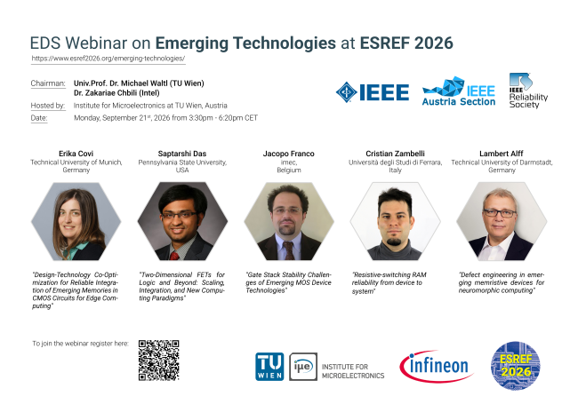
[EDS Webinar] Emerging Technologies at ESREF 2026


IEEE EDS Webinar Series

Emerging Technologies at ESREF 2026


Sponsored By: The IEEE Electron Devices Society Educational Activities Committee and Device Reliability Physics Committee

The EDS Webinar on Emerging Technologies, held within ESREF 2026 at TU Wien in Vienna, will address recent developments and reliability challenges in emerging device technologies. Topics include 2D FETs, advanced MOS gate stacks, emerging and resistive-switching memories, and memristive devices for neuromorphic computing, covering aspects from device-level reliability and defect engineering to CMOS integration and system-level considerations.


Date: 21 September 2026


Time: 9:30 AM - 12:20 PM EDT / 3:30 - 6:20 PM CEST
(
Time Zone Conversion Tool)


Presenters: Dr. Erika Covi, Dr. Saptarshi Das, Dr. Jacopo Franco, Dr. Cristian Zambelli, Dr. Lambert Alff


More Information Here

This message is being sent on behalf of the EDS Vice President of Educational Activities, P Susthitha Menon


As part of our commitment to advancing the vision and mission of the Electron Devices Society, we are pleased to invite you to attend our next scheduled webinar.


All participants will receive virtual meeting details prior to the event. We sincerely hope that you can join us for this event.

Register to Join Virtually
Facebook  X  Instagram  LinkedIn