Apr 30, 2024

[Kick-off] Chipdesign Germany

Chipdesign Germany
Das Netzwerk für Chipdesign in Deutschland
https://www.chipdesign-germany.de/
OnLine Registrierung: https://eveeno.com/auftaktchipdesigngermany

Juni 6. Donnerstag
13:00 Ankunft & Registrierung
14:00 Eröffnung
14:00 Begrüßung
Holger Blume; Leibniz Universität Hannover & edacentrum e.V.
14:15 Grußworte
Apollonia Pane Bundesministerium für Bildung und Forschung 
14:30 Vorstellung Chipdesign Germany
Holger Blume; Leibniz Universität Hannover & edacentrum e.V.
Norbert Wehn; Rheinland-Pfälzische Technische Universität Kaiserslautern-Landau
14:45 Keynote-Session I
14:45 Open-Source EDA and Innovation Leadership
Andrew B. Kahng; University of California San Diego, US
15:45 Kaffeepause
16:30 Keynote-Session II
16:30 Open Source Chip Design: Europas Weg zur Wettbewerbsfähigkeit in einer geteilten Tech-Welt?
Jan-Peter Kleinhans; Stiftung Neue Verantwortung
17:30 Mikroelektronik in digitalen Hörhilfen: Chips, die hören helfen
Joachim Thiemann; Advanced Bionic
18:30 Networking-Veranstaltung mit Poster- & Demo-Session

Juni 7. Freitag
08:30 Eröffnung
08:30 Begrüßung
Holger Blume; Leibniz Universität Hannover & edacentrum e.V
08:45 Keynote-Session III
08:45 Neue Fertigungstechnik für die Chipverarbeitung
Lutz Rissing; Dr. Johannes Heidenhain GmbH
09:45 Kaffeepause
10:30 DE:Sign Präsentationen
BMBF-Förderlinie "Design-Instrumente für souveräne Chipentwicklung mit Open-Source (DE:Sign)"
10:30 DI-OCRCpro
Daniel Krupka; Gesellschaft für Informatik e.V.
10:45 DI-DEMICO
Frank Ellinger; Technische Universität Dresden
11:00 DI-DERAMSys
Matthias Jung; Julius-Maximilian-Universität Würzburg
11:15 DI-OWAS
Dirk Koch; Ruprecht-Karls-Universität Heidelberg
11:30 DI-PASSIONATE
Robert Weigel; Friedrich-Alexander Universität Erlangen-Nürnberg
11:45 Interaktive Poster-Session
13:30 Verabschiedung

Adresse: Königlicher Pferdestall - Leibniz Universität Hannover; Appelstr. 7, 30167 Hannover
OnLine Registrierung: https://eveeno.com/auftaktchipdesigngermany


Workshop on Advanced Integrated Circuit Design

U.S.-Japan Collaborative Workshop on Advanced Integrated Circuit Design
(Phase 2)
Fukuoka System LSI Development Center 2F
May 14 - May 15, 2024
https://www.kerc.or.jp/seminar/2024/04/5145152.html

In recent years, R&D and investment in semiconductors have become more active in countries around the world, and at the same time, the need for human resource development has been pointed out. In Japan in particular, the construction and attraction of factories for semiconductor "manufacturing" is accelerating, and various activities are being developed, but in the future, it is necessary to accelerate discussions on semiconductor "design". Against this backdrop, with the support of the U.S. Consulate in Fukuoka, we decided to hold a workshop in collaboration with the U.S. In December 2023, we held the U.S.-Japan Collaborative Workshop on Circuit Design (Phase 1), a state-of-the-art integrated circuit design, with the aim of learning about the latest situation in both countries through lectures on cutting-edge design technology and human resource development in Japan and the United States, as well as discussing the future direction and possibilities for international collaboration. We cover a wide range of topics, including open IC design, advanced analog and digital circuit design, generative AI processing (LLM) acceleration, optical circuit design, cryogenic classical and quantum computing, and new device technologies. Hybrid format (lectures can be held at Fukuoka venues and ZOOM Webinars), free of charge, with simultaneous English-Japanese interpretation. Therefore, it is a form that is easy to participate in. This is a good opportunity to learn about global trends, so not only those who specialize in semiconductors, but also those who are even a little interested in semiconductors, please join us. Students are also welcome to participate! In addition, we plan to have a simple hands-on session in the tutorial session, so if you are interested, please bring / prepare a laptop.

Outline of the event

Date & Time
DAY-1: May 14, 2024 10:00 a.m. ~ 4:00p.m.
DAY-2: May 15, 2024 10:00 a.m. ~ 4:05 p.m.

Hybrid format (lectures can be held at Fukuoka venues and ZOOM Webinars)
Online (Zoom Webinars)

Fukuoka Venue: Fukuoka System LSI Development Center 2F
(〒814-0001 3-8-33 Momochihama, Sawara-ku, Fukuoka City)
There is no parking lot at the venue, so if you come by car, please use the
nearby paid parking lot.

Participation Fee:  free

Application
[Application deadline: May 13]
Please apply from the link below (you can also apply for either Day-1 or Day-2 only). Simultaneous interpretation in English and → is available at the Fukuoka venue and ZOOM Webinars. The first 70 people to participate at the Fukuoka venue and the first 400 people to participate in the ZOOM Webinar will be closed to the first 400 people. If you wish to cancel after applying for the Fukuoka venue, please contact us as soon as possible. In addition, we are planning a simple hands-on, so please bring your laptop (you can participate without a laptop).

Application Form

Program Details  (subject to update) https://www.kerc.or.jp/seminar/2024/04/5145152.html

Day-1: May 14, 10:00-16:00 (JST)

10:00 - 10:05 Opening Remark and Overview of the Workshop, Mehdi Saligane/Koji Inoue, University of Michigan/Kyushu University
[Morning Session: Invited Talks]
10:05 - 10:10 Welcome Remarks from the U.S. Consulate in Fukuoka
10:10 - 10:55 LLMs on ASICs, Greg Kielian/Kauna Lei, Google Research
11:00 - 11:45 Teaching Mixed-Signal Design Using Open-Source Tools, Boris Murmann, University of Hawaii
11:45 - 13:00 Lunch Break
[Afternoon Session: Tutorials]
13:00 - 14:00 Photonic and Analog circuits with GDSFactory, Joaquin Matres/Troy Tamas, Google X/DoPlayDo, Inc.
14:00 - 14:15 Break
14:15 - 15:45 ReaLLMASIC: Build your own Lightweight LLM, Gregory Kielian/Kauna Lei/Shiwei Liu/Mehdi Saligane, Google Research/University of Michigan
15:45 - 16:00 Conclusion, Mehdi Saligane, University of Michigan

Day-2: May 15th, 10:00-16:05 (JST) 
10:00 - 10:05 Opening Remark and Overview of Day-2 Workshop, Mehdi Saligane/Koji Inoue, University of Michigan/Kyushu University
[Morning Session: Invited Talks]
10:05 - 10:50 Superconductor Computer Architecture: from Classical to Quantum, Ilkwon Byun, Kyushu University
10:50 - 11:35 Overview of new devices in the era of Beyond CMOS, Sadayuki Yoshitomi, Megachips
11:35 - 13:00 Lunch Break
[Afternoon Session: Tutorials]
13:00 - 13:55 (Tentative: GLayout), Anhang Li/Boris Murmann/Mehdi Saligane, University of Michigan/University of Hawaii
13:55 - 14:50 (Tentative: XLS: High-Level Synthesis), Johan Euphrosine, Google
14:50 - 15:05 Break
15:05 - 16:00 Pitfalls of Open-Source Chip Design Verification, Mitch Bailey, Efabless/ShuhariSystem
16:00 - 16:05 Conclusion and Overview of the phase-2 workshop activities, Mehdi Saligane/Koji Inoue, University of Michigan/Kyushu University


Organizer
University of Michigan
Kyushu University System LSI Research Center Kyushu University
Quantum Computing Systems Research Center Kyushu University
Value Creation Semiconductor Human Resource Development Center

Co-organizers
Fukuoka Prefectural Foundation for the Promotion of Industry, Science and Technology Kyushu Economic Research Association

Sponsor
U.S. Consulate in Fukuoka

Inquiries
ic-design-ws 'at' slrc.kyushu-u.ac.jp (replace 'at' with @)
Okano, Business Development Department, TEL: 092-721-4907

Apr 29, 2024

In Memoriam: Willy Sansen (1943-2024)

In Memoriam: Willy Sansen (1943-2024)
// by caeleste.be/

We are deeply saddened to announce the passing of Willy Sansen, Emeritus Professor of Engineering Science at KU Leuven and esteemed member of the Board of Directors at Caeleste.

With heavy hearts, we say farewell to a true visionary and leader in the field of engineering. Throughout his distinguished career, Willy's contributions to both academia and industry were immeasurable.

As a professor, he inspired generations of students with his passion for research and teaching. As a member of our board, his guidance and expertise were instrumental in shaping the direction of Caeleste.

Willy's legacy will forever endure through the lives he touched and the knowledge he shared. Our thoughts are with his family and loved ones during this difficult time.

Rest in peace, Willy Sansen.
Your impact will continue to inspire us all.


Apr 26, 2024

[paper] Compact Modeling of Hysteresis in OTFTs

Compact modeling of hysteresis in organic thin-film transistors
A. Romeroa, J.A. Jiménez-Tejadaa, R. Picosb, D. Laraa, J.B. Roldána, M.J. Deenc
Organic Electronics 129 (2024) 107048
DOI : 10.1016/j.orgel.2024.107048

a Departamento de Electrónica y Tecnología de Computadores, CITIC-UGR, Uni Granada, Spain
b Department of Industrial Engineering and Construction, Universitat de les Illes Balears, Spain
c Department of Electrical and Computer Engineering, McMaster University, Canada


Abstract: In this work, we propose a model that describes the temporal evolution of the threshold voltage and trapped charge density in Thin-Film Transistors (TFTs) under dynamic conditions, paving the way for the characterization and modeling of memory transistors. The model is expressed as a first-order differential equation for the trapped charge density, which is controlled by a time constant and an independent term proportional to the drain current. The time-dependent threshold voltage is introduced in a previously developed compact model for TFTs with special consideration to the contact effects. The combination of both models and the use of an evolutionary parameter extraction procedure allow for reproducing the experimental dynamic behavior of TFTs. The results of the model and the evolutionary procedure have been validated with published experimental data of pentacene-based transistors. The procedure is able to simultaneously reproduce three kinds of experiments with different initialization routines and constraints in each of them: output and transfer characteristics with hysteresis and current transients characteristics
FIG: a.) Modeling the contact regions and intrinsic channel of an OTFT structure (a bottom contact configuration); b.)  Comparison of experimental transfer characteristics


Acknowledgements : The authors acknowledge support from the project PID2022 139586NB-44 funded by MCIN/AEI/10.13039/501100011033 and FEDER, EU. Funding for open access charge: Universidad de Granada / CBUA.

Appendix: Supplementary material related to this article can be found online.

Apr 25, 2024

[PhD] Transient Simulation of Frequency Domain Devices in Gnucap

Adding transient simulation of frequency domain devices to the Gnucap circuit simulator
Phd Thesis by Seán Higginbotham
Supervisor: Assistant Prof. Justin King
April 2024
Trinity College Dublin, The University of Dublin
College Green, Dublin 2, Ireland

Abstract: Radio frequency design constitutes a dominant element in the development of key communications technologies. Having accurate, robust, and widely accessible simulation methods is critical to ensuring continued advancements in this field, and guaranteeing the associated infrastructural and societal shifts that such technologies enable.
High frequency circuits invariably contain multiple non-linear components, which are naturally dealt with via time marching simulation of their time-domain analytic equations. However, including this alongside linear, generally dispersive, devices and effects, which are typically only characterised through a set of frequency-domain data describing the scattering response of an associated port-network, has traditionally been a problem for designers. Frequency-domain methods such as the harmonic balance technique and its successors have dominated radio frequency design for decades. However, such methods exhibit disadvantages in the context of modern circuits which are increasingly non-linear, and which operate with increasingly complicated modulated signals.
Various alternatives have been proposed, though as of yet no universally accepted method has emerged. Though harmonic balance will likely not be replaced, this project seeks to implement one such pure transient technique as an alternative. The proposed technique is based on using the vector-fitting algorithm to produce a model of the frequency response of the linear portnetwork, and then using a recursive convolution formulation to allow the time-domain response to be efficiently obtained from the port’s impulse response. An equivalent circuit companion model is developed from the resulting time-domain power-wave relation. This companion model allows the linear device to be directly included in a transient simulation alongside the analytic non-linear components, by way of providing a manner of computing the voltage and current on the network’s ports.
We implement the technique for one-port networks in a circuit driven by baseband signals. It is added to the free, open-source Gnucap circuit simulator as a ‘device plugin’. This report details how the implementation was done and provides results illustrating that it works as intended; the plugin can be installed by a user, who simply provides it with a file of frequency-domain data representing the port-network, and the plugin works naturally with the Gnucap transient solver to allow obtaining a transient solution of the overall circuit. A pure transient technique such as this does not require limiting assumptions or approximations on any components in the circuit and they are therefore preferable in certain contexts to frequency-domain methods like harmonic balance.
The project offers a significant contribution towards increasing the accessibility of radiofrequency electronics design and teaching.

 FIG: Summary of the traditional approach to simulating RF/MW circuits via HB, and the proposed pure transient approach implemented in this PhD Thesis

Acknowledgements: Seán Higginbotham would like to thank my M.A.I supervisor Dr. Justin King, whose previous work was the basis for this project. He provided invaluable insights and guidance which made the project both possible and an enjoyable experience, instilling curiosity at each discussion. Relevant academic references are included in the bibliography section. Acknowledgements of the dependancies used in the project code follow.

Gnucap is the creation of Albert Davis and is developed by him and others. It is provided under the GNU GPLv3, which is also the license that this project code is provided under on the associated GitHub repository.
See https://www.gnu.org/licenses/gpl-3.0.html. For the GNU GPLv3 license. Additionally, see the Gnucap repository here https://savannah.gnu.org/projects/ gnucap/.

LAPACK is a co-creation of The University of Tennessee and The University of Tennessee Research Foundation, The University of California Berkeley, and The University of Colorado Denver. See the user guide here https://netlib.org/lapack/.
The LAPACKE C bindings are the creation of Intel Corp.

The relevant licensing files are found within the source code and on the respective website.

Should the reader of this report have any questions or suggestions, please feel free to reach out at higginbs@tcd.ie, or via other channels such as the project GitHub located at https: //github.com/SHigginbotham/transient-sparam-gnucap. The project supervisor may also be of interest, available at justin.king@tcd.ie.

[paper] Flexible TFT Electronics

Hikmet Çeliker, Wim Dehaene and Kris Myny
Multi-project wafers for flexible thin-film electronics by independent foundries.
Nature (2024)
DOI: 10.1038/s41586-024-07306-2

1. ESAT, KU Leuven, Leuven, Belgium
2. imec, Leuven, Belgium

Abstract: Flexible and large-area electronics rely on thin-film transistors (TFTs) to make displays large-area image sensors, microprocessors, wearable healthcare patches, digital microfluidics, and more. Although silicon-based complementary metal–oxide–semiconductor (CMOS) chips are manufactured using several dies on a single wafer and the multi-project wafer concept enables the aggregation of various CMOS chip designs within the same die, TFT fabrication is currently lacking a fully verified, universal design approach. This increases the cost and complexity of manufacturing TFT-based flexible electronics, slowing down their integration into more mature applications and limiting the design complexity achievable by foundries. Here we show a stable and high-yield TFT platform for the fabless manufacturing of two mainstream TFT technologies, wafer-based amorphous indium–gallium–zinc oxide and panel-based low-temperature polycrystalline silicon, two key TFT technologies applicable to flexible substrates. We have designed the iconic 6502 microprocessor in both technologies as a use case to demonstrate and expand the multi-project wafer approach. Enabling the foundry model for TFTs, as an analogy of silicon CMOS technologies, can accelerate the growth and development of applications and technologies based on these devices.

FIG:  Photograph of all three chips at once: the vintage WDC 65C02 in a 40-pin DIP package (left), the flex LTPS 6502 (middle) and the flex IGZO 6502 (right)


Acknowledgements: We thank PanelSemi (a system-on-film foundry service provider in Taiwan) for providing LTPS panels and Pragmatic for providing IGZO wafers as a verification of our designs, using their foundry-mode panel and wafer delivery services. Part of this work has received funding under the Horizon Europe programme from the European Research Council under grant agreement no. 101088591 ‘ORISON project’. Views and opinions expressed are, however, those of the authors only and do not necessarily reflect those of the European Union or the European Research Council. Neither the European Union nor the granting authority can be held responsible for them.

Apr 22, 2024

[C4P] Orbitaly2024 in Bologna

8th International Conference on Organic Bioelectronics
Orbitaly2024
Bologna Sept. 23-25, 2024

OrBItaly (Organic BIoelectronics Italy) is an international conference, organized by the Italian scientific community and dedicated to the most recent results in the field of bioelectronics, with a particular focus on the employment of organic materials. OrBItaly has attracted in the years a growing interest of the scientists coming from all over the world. The 2024 edition is the seventh one of this cross-disciplinary conference, and will be held in Bologna, on September 23rd-25th, 2024, at the San Giovanni in Monte historic building in the centre of Bologna.

The abstract submission is open, with its deadline on 15th June 2024. 

All details about the conference can be found on the website: https://eventi.unibo.it/orbitaly2024

Looking forward to meeting you in Bologna

The OrBItaly 2024 Organizing Committee
Beatrice Fraboni, 
Francesco Decataldo, 
Marta Tessarolo, 
Tobias Cramer,
Vito Vurro


Apr 21, 2024

[webinar] Open Source EDA Development of Chips in Europe

Professor Marie-Minerve Louerat, Sorbonne Université-CNRS, GoIT Project, has announced the upcoming webinar on Open Source EDA fostering development of Chips in Europe


"Introduction to the open-source EDA ecosystem"
online webinar to foster engagement for Open-Source EDA and Open-Silicon development in Europe

📅 Tuesday May 14, 2024 🕙 10:00-12:00 (CEST) with Free Online Registration

Workshop Agenda:
  • European Semiconductor Design Ecosystem (10 min)
    • Matthew Xuereb, European Commission
  • Open-Source Semiconductor Ecosystem (15 min)
    • Luca Alloatti, Free Silicon Foundation (I) ETS
  • Open-Source EDA Software and Semiconductor Design (15 min)
    • Jean-Paul Chaput, Sorbonne Université, Coriolis Foundation
  • European Roadmap on the Advancement of Open-Source EDA Tools, next steps (15 min)
    • Rihards Novickis, Latvian Institute of Electronics and Computer Science
  • Q&A session / Feedback (up to 1 hour)
NB: 2nd event - to be announced
Location: Paris, Sorbonne Université
📅 Date: June 18, 2024, before FSiC2024 conference


Apr 18, 2024

[IEEE SSCS] “PICO” Open-Source Chipathon

IEEE SSCS “PICO” Open-Source Chipathon
Automating Analog Layout
– Sign-Up Deadline: May 10, 2024 –

The IEEE Solid-State Circuits Society is pleased to announce its fourth open-source integrated circuit (IC) design contest under the umbrella of its PICO Program (Platform for IC Design Outreach). While this contest is open to anyone (no restrictions), we encourage the participation of pre-college students, undergraduates, and geographical regions that are underrepresented within the IC design community. 


The goal of this year’s event is to advance the automatic generation and open sharing of analog circuit layout cells to increase our community’s design productivity and to catch up with other fields where sharing and automation is a key enabler of progress (e.g., in machine learning).

Die photo in background courtesy of IBM

Contest Outline

  1. Interested individuals sign up using this form by May 10, 2024.
  2. Phase 1 (~June): Through a series of weekly meet-ups and training sessions, the participants learn to create basic one- or two-transistor layout generators using Python and open-source CMOS PDKs. Using Jupyter Notebooks hosted on Google Colab allows anyone with an internet connection to participate - no downloads or installations required! Relevant circuit examples can be found in [1], [2]. We will leverage code modules available with the OpenFASoC [3] environment.
  3. Phase 2 (~July): Interested participants define larger layout building blocks that they wish to automate (examples: comparator, bandgap, phase interpolator, OTA). Teaming among participants is encouraged to maximize collaboration and learning).
  4. Phase 3 (~August-September): Participants implement their generators and submit sample layouts and test structures for potential tape-out to an open-source MPW (tentatively SKY130).
  5. Phase 4 (~October-November): A jury evaluates the created generators/layouts and selects the test structures that will be taped out. The teams work together to assemble a shared database with all the designs and to complete the tapeout. Ideally, this phase will involve automated verification through CACE [4] or a similar tool.
  6. Phase 5 (TBD): The designs will be tested using lab measurements by a subset of participants and SSCS volunteers with access to lab facilities. Some of the test setups may be available for remote characterization. The obtained measurement data will be added to the repositories containing the layout generators.

 References

[1] H. Pretl, “Fifty Nifty Variations of Two-Transistor Circuits,” MOS-AK Workshop Spring 2022, URL: https://www.mos-ak.org/spring_2022/presentations/Pretl_Spring_MOS-AK_2022.pdf.
[2] H. Pretl and M. Eberlein, "Fifty Nifty Variations of Two-Transistor Circuits: A tribute to the versatility of MOSFETs," in IEEE Solid-State Circuits Magazine, vol. 13, no. 3, pp. 38-46, Summer 2021, URL: https://ieeexplore.ieee.org/document/9523464.
[3] OpenFASoC: Fully Open-Source Autonomous SoC Synthesis using Customizable Cell-Based Synthesizable Analog Circuits, https://github.com/idea-fasoc/OpenFASOC/.
[4] Circuit Automatic Characterization Engine, URL: https://github.com/efabless/cace.

Apr 16, 2024

[paper] SiC Power MOSFET SPICE modelling

Akbar Ghulam
Accurate & Complete behaviourial SPICE modelling 
of commercial SiC Power MOSFET OF 1200V, 75A
25th EuroSimE, Catania, Italy, 2024, pp. 1-4,
DOI: 10.1109/EuroSimE60745.2024.10491420

* UNIPA Palermo (IT)

Abstract: Silicon Carbide (SiC) is proved to be an excellent replacement for Silicon in high voltage and high frequency applications due to its electro-thermal properties. Since SiC power MOSFETs have only recently been more widely available commercially, accurate simulation models are immediately required to forecast device behavior and facilitate circuit designs. The goal of this paper is to develop an accurate LTSPICE model based on a modified Enz-Krumenacher-Vittoz (EKV), MOSFET model for a 1200V, 30mΩ & 75ASiC power MOSFET “SCTW100N120G2AG” provided by STMicroelectronics that is currently on the market. The modified EKV model outperforms the reduced quadratic model by describing MOSFET behavior over different zones which are weak, moderate, and strong inversion zones with only a single equation. A wide range of experimental data was used to build the model's parameters. To estimate device performance in high frequency switching applications, the model has been expanded to include package parasitic components that include parasitic capacitances. The model's static and transient properties were simulated, and the results were compared with those acquired from the actual device.
FIG: The SiC MOSFET's circuit schematic utilizing a modified EKV model

Acknowledgements: We would like to thank STMicroelectronics, as for completion of this study has been greatly aided by their participation and availability of relevant data.

Apr 15, 2024

[course] MEAD @ EPFL

Live Course @ EPFL, Lausanne, Switzerland
JUNE 17-21, 2024

Registration Deadline: May 17, 2024 >> REGISTER

MONDAY, June 17

8:30 am-12:00 pmMOS Transistor Modeling for Low-Voltage and Low-Power Circuit DesignChristian Enz
1:30-5:00 pmDesign of Low-Power Analog Circuits using the Inversion CoefficientChristian Enz

TUESDAY, June 18

8:30 am-12:00 pmNoise Performance of Elementary Circuit BlocksBoris Murmann
1:30-5:00 pmOpamp Topologies and Design FundamentalsBoris Murmann

WEDNESDAY, June 19

8:30-10:00 amLow-Power High Efficiency OpAmp DesignKlaas Bult
10:30 am-12:00 pmLow-Power High Efficiency Residue AmplifiersKlaas Bult
1:30-3:00 pmAnalog Design Methodology and Practical Techniques for Frequency CompensationVadim Ivanov
3:30-5:00 pmEnergy Efficient Voltage References, Biasing in Analog Systems and Current SourcesVadim Ivanov

THURSDAY, June 20

8:30-10:00 amPower Dissipation in ADC Buidling BlocksKlaas Bult
10:30 am-12:00 pmPower Dissipation in ADCsKlaas Bult
1:30-5:00 pmMicropower ADCsKofi Makinwa

FRIDAY, June 21

8:30 am-12:00 pmEnergy Efficient Sensor InterfacesTaekwang Jang
1:30-5:00 pmLow-Power Frequency Reference CircuitsTaekwang Jang
1:30-5:00 pmPower Management With Nanoampere Consumption and Efficient Energy HarvestingVadim Ivanov

Apr 14, 2024

GDR SOC2 IEEE CASS

GDR SOC2 - IEEE CASS
“Tour de France” - Grenoble - 19 April 2024
Open Hardware: the new road?
INP; 46 Av Felix Viallet 38000 Grenoble – Amphi Gosse

8:30  Prof. Boris Murmann (U. of Hawaii) 
Re-Energizing Analog Design using the Open-Source Ecosystem. 
9:30  Aurélien Nicolet (CIME-P)
The French platform supporting open hardware
10:00 Krzysztof Herman (IHP)
 IHP Open Source PDK -  sharing experience after one year of development.
11:00 75th anniversary of CAS Society Keynote by Prof. Ricardo Reis.
12:00 Lunch & Cocktail
14:00 Prof. Ricardo Reis (UFRGS)
 Why joining IEEE CAS Society?
14:30 Jean-Paul Chaput (LIP6 – Sorbonne University)
 Coriolis, The European Open Hardware Project 
15:30 Dr. Leonardo Gomes (TIMA - UGA)
 The first 60 GHz circuit designed with open hardware platform
16:00 Deni Alves (UFSC)
 ACM, a design-oriented model for open tools

Inscription Gratuite: à laurence.ben-tito@univ-grenoble-alpes.fr  


Apr 12, 2024

[paper] Heterojunction Nano-HEMT

G. Purna Chandra Rao1, Trupti Ranjan Lenka2, Valeria Vadalà3
and Hieu Pham Trung Nguyen4
Characteristics Study of Heterojunction III-Nitride/β-Ga2O3 Nano-HEMT for THz Applications
Eng. Res. Express (2024) in press
DOI: 10.1088/2631-8695/ad3db1

1 Electronics and Communication Engineering, NIT Silchar, Assam (IN)
2 Electronics and Communication Engineering, NIT Silchar, Assam (IN)
3 Physics, University of Milan-Bicocca (IT)
4 Electrical and Computer Engineering, Texas Tech University (USA)

Abstract: In this research study, a recessed gate III-Nitride high electron mobility transistor (HEMT) grown on a lattice matched β-Ga2O3 substrate is designed. This research investigation aims to enhance DC and RF performance of AlGaN/GaN HEMT, and minimize the short-channel effects by incorporating an AlGaN back layer and field plate technique, which can enhances electron confinement in two-dimensional electron gas (2DEG). A precise comparison analysis is done on the proposed HEMT’s input characteristics, output characteristics, leakage current characteristics, breakdown voltage properties, and RF behaviour in presence and absence of AlGaN back layer in regard to field plate configuration. The inclusion of back barrier aids in raising the level of conduction band, which reduces leakage loss beneath the buffer, and aids in keeping the 2DEG to be confined to a narrow channel. Furthermore, the field plate design offers an essential electric field drift between gate and drain, resulting to enhanced breakdown voltage characteristics.
FIG : Epitaxial schematic illustration of suggested III-nitride HEMT with the proposed back barrier and field plates.

Acknowledgment : The authors acknowledge SERB (Science and Engineering Research Board), Govt. of India sponsored Mathematical Research Impact Centric Support (MATRICS) project no. MTR/2021/000370 for support.


Apr 8, 2024

[Symposium] SFRC AIST

Advanced Semiconductor Research Center (SFRC) 
National Institute of Advanced Industrial Science and Technology (AIST)
1st Open Symposium 
https://unit.aist.go.jp/sfrc/sfrcsympo202405.html

Date: May 27, 2024
Venue: Fujisoft Akiba Plaza Akiba Hall (3 Kanda-Neribaki-cho, Chiyoda-ku, Tokyo) 
Hybrid event (on-site participation and remote streaming)

AGENDA:
Moderator: Takashi Matsukawa (Deputy Director, SFRC)
13:00-13:05 Opening Remarks Tetsuji Yasuda (AIST Electronics & Manufacturing)
13:05-13:10 Guest Greetings Mr. Tsutomu Kanashi (Director, Information Industry Division, Commerce and Information Policy Bureau, Ministry of Economy, Trade and Industry)
13:10-13:40 Keynote Speech 1 "Rapidus and Advanced Semiconductor Development" Masaharu Kobayashi (Rapidus Corporation)
13:40-14:10 Keynote Speech 2 "The Current Situation and Future of the Semiconductor Industry from a Systems Perspective" Kenji Tsuda (International Technology Journalist)
14:10-14:20 "Introduction to the Advanced Semiconductor Research Center" Akiue Masahara (Director, SFRC Research Center)
14:20-14:40 "Introduction of SCR Open Pilot Line" Fuminori Ito (Deputy Director, SFRC)
14:40-14:55 "2nm Generation GAA-FET Fundamental Technology" Hisashi Irizawa (SFRC) Head, Device Process Research Team)
14:55-15:10 "Extreme Device and Material Technology for the 2nm Generation and Beyond" Naoya Okada (Head, Extreme CMOS Materials Research Team, SFRC)
15:10-15:30 Coffee Break
15:30-16:00 Keynote Speech 3 "What is Open Source Utilized Silicon Initiatives (Open-SUSI)?" Jun-Ichi Okamura (AIST Solutions)
16:00-16:15 "Device Integration Technology by 3D Integrated Packaging Technology Katsuya Kikuchi (Director, SFRC 3D Integrated Technology Research Team)
16:15-16:30 "Advanced System-on-Chip (SoC) Design Technology"
Shinichi Ouchi (AIDL Laboratory Team Leader/SFRC Integrated Circuit Design Research Team)
16:30-16:45 Environmental Impact Assessment of Semiconductor Manufacturing and Greening Technologies" Shinji Mimida (SFRC)
16:45-17:00 "Quantum-related semiconductor integrated device technology" Takahiro Mori (Director, SFRC New Principles Silicon Device Research Team)
17:00-17:15 Q&A
17:15-17:30 Closing Remarks Takashi Nakano (Deputy Director, Research Strategy Planning Department, AIST)

On-site participation, remote participation: Participation is free. (Please register for this form) Remote streaming is scheduled for Zoom. Please register one by one if you wish to participate. Please note that there is a limit to the number of participants at the venue.

Secretariat contact <https://unit.aist.go.jp/sfrc/sfrcsympo202405.html>
National Institute of Advanced Industrial Science and Technology (AIST) Advanced Semiconductor Research Center Symposium Secretariat (M-SFRC-Sympo-ml@aist.go.jp)

Apr 5, 2024

[paper] Organic Electrochemical Transistor Arrays

Jaehyun Kim, Robert M. Pankow, Yongjoon Cho, Isaiah D. Duplessis, Fei Qin, Dilara Meli, Rachel Daso, Ding Zheng, Wei Huang, Jonathan Rivnay, Tobin J. Marks and Antonio Facchetti
Monolithically integrated high-density vertical organic electrochemical transistor arrays
and complementary circuits.
Nat Electron 7, 234–243 (2024)
DOI: 10.1038/s41928-024-01127-x

1 Department of Chemistry and Materials Research Center, Northwestern University, Evanston, IL, USA
2 Department of Semiconductor Science, Dongguk University, Seoul, Republic of Korea
3 Department of Materials Science and Engineering, Northwestern University, Evanston, IL, USA
4 Department of Biomedical Engineering, Northwestern University, Evanston, IL, USA
5 Laboratory of Organic Electronics, Department of Science and Technology, Linköping University, Sweden
6 School of Materials Science and Engineering, Georgia Institute of Technology, Atlanta, GA, USA


Abstract Organic electrochemical transistors (OECTs) can be used to create biosensors, wearable devices and neuromorphic systems. However, restrictions in the micro- and nanopatterning of organic semiconductors, as well as topological irregularities, often limit their use in monolithically integrated circuits. Here we show that the micropatterning of organic semiconductors by electron-beam exposure can be used to create high-density (up to around 7.2 million OECTs per cm2) and mechanically flexible vertical OECT arrays and circuits. The energetic electrons convert the semiconductor exposed area to an electronic insulator while retaining ionic conductivity and topological continuity with the redox-active unexposed areas essential for monolithic integration. The resulting p- and n-type vertical OECT active-matrix arrays exhibit transconductances of 0.08–1.7 S, transient times of less than 100 μs and stable switching properties of more than 100,000 cycles. We also fabricate vertically stacked complementary logic circuits, including NOT, NAND and NOR gates.
FIG: High-density monolithically integrated vOECT arrays fabricated by e-beam exposure.
 a.) Photograph  vOECT arrays comprising bgDPP-g2T OECTs
b.) Transconductance map of the wafer-scale vOECTs; 
c.) Transfer IVs of 100 bgDPP-g2T vOECTs (W = d = 10 µm) 

Acknowledgements: This work was supported by the AFOSR (contract no. FA9550-22-1-0423), the US Office of Naval Research Contract no. N00014-20-1-2116, by the US Department of Commerce, National Institute of Standards and Technology as part of the Centre for Hierarchical Materials Design Award no. 70NANB10H005, BSF (award no. 2020384), NSF (DMR-2223922) and the Northwestern University Materials Research Science and Engineering Center Awards NSF DMR-1720139 and DMR-2308691. J.R. gratefully acknowledges support from the Alfred P. Sloan Foundation (FG-2019-12046). This work acknowledges the US Department of Energy under contract no. DE-AC02-05CH11231 at beamline 8-ID-E of the Advanced Photon Source, a US Department of Energy (DOE) Office of Science User Facility operated for the DOE Office of Science by Argonne National Laboratory under Contract No. DE-AC02-06CH11357. This work made use of the NUFAB facility of Northwestern University’s NUANCE Center, which has received support from the SHyNE Resource (NSF ECCS-2025633), the IIN and Northwestern’s MRSEC programme (NSF DMR-1720139).

Apr 3, 2024

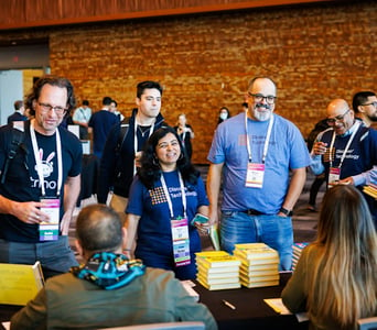
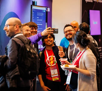
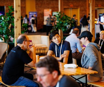
[Linix Foundation] Open Source Summit: April 16-17


OSSNA 1
OSSNA 2
OSSNA 3

Hi WS, 


Open Source Summit North America starts in just 2 weeks - April 16-18 in Seattle, WA! 

The Schedule is PACKED.


We've got it all: 200+ sessions across 16 microconferences. From Linux to AI, Security, Cloud, Containers, OSPOs, and beyond. It's an all-you-can-learn buffet on today's most vital open source tech and topics.

What's NEW at OSS?

  • Lunch is now included in registration letting attendees stay onsite and get even more time for networking & collaboration.

  • Unconference Track: Have a topic you would like to discuss? Sign up onsite to schedule your talk.

  • AI-powered Networking App & Speed Networking, making it easier to find the right connections.

  • Access to Embedded Open Source Summit offering another 200 sessions at no added cost.

  • 3 NEW Microconferences: Digital Trust, Standards & Specification Forum and TechDocsCon.

  • LFX Mentorship Showcase: Hear from LF Mentorship Program mentees, recruit new talent, and support new developer contributions. Learn more here.

Register Now!


Register by April 7 and SAVE. Don't delay - prices go UP on April 8. 


Reduced registration fees are available starting at $275 for academics, government, hobbyist and $500 for small business. Review all registration types here

Don't Let Time Run Out!

Don't miss the chance to join the leading event for open source developers, technologists, and community leaders, with content for developers, system operators and community, across a wide range of topics, subjects, and skill levels.


See you in Seattle!

Thank You to Our Sponsors!

DIAMOND:

PLATINUM:

GOLD:

SILVER:

BRONZE:

This email was sent by: The Linux Foundation Events

548 Market St, PMB 57274, San Francisco, CA 94104-5401, United States

Subscription Center