Jun 4, 2020

[paper] On-Wafer FinFET-Based EUV/eBeam Detector Arrays

Wang, Chien-Ping, Yi-Pei Tsai, Burn Jeng Lin, Zheng-Yong Liang, Po-Wen Chiu, Jiaw-Ren Shih, Chrong Jung Lin, and Ya-Chin King
On-Wafer FinFET-Based EUV/eBeam Detector Arrays for Advanced Lithography Processes
IEEE TED (2020)

Abstract: A novel microdetector array (MDA) for monitoring electron beam (eBeam) and extreme ultraviolet (EUV) lithography processes in 5 nm and beyond FinFET technology is first-time presented. This on-wafer detector array consists of high-density sensing cells which are fully compatible with standard FinFET CMOS processes. Fin coupling structures and energy-sensing pads are first applied in an ultrasmall detector for realizing efficient eBeam and EUV photon detection. In advanced lithography process, eBeam or EUV level projected on the wafer can be precisely recorded on the on-wafer MDA without power or batteries. The distributions and variations on the beam intensities collected by MDA can be electrically measured in real time or inline through wafer level test after eBeam or EUV exposures. The proposed MDA is expected to provide real-time feedback for the optimization and stable maintenance of advanced photolithography processed critical to the development nanometer CMOS technologies.
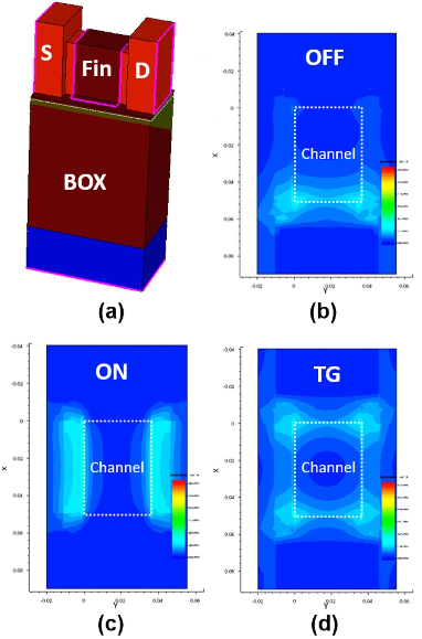
FIG: (a) Schematic of lithography system and (b) 3-D illustration of unit detector cell of the MDA consisting of ESP and FG on the shallow trench isolation (STI) region.

Acknowledgment: The authors gratefully acknowledge the contributions of Taiwan Semiconductor Manufacturing Company (TSMC) and Ministry of Science and Technology (MOST), Taiwan (Project Number: MOST 108-2622-8-007-017).


Jun 2, 2020

IEEE EDS Delhi Chapter DL: FOSS TCAD/EDA tools for Compact/SPICE Modeling

The IEEE EDS Delhi Chapter, New Delhi, India is conducting a series of the IEEE EDS DL Talks with coming one on June 03, 2020 at 06:00 pm (GMT+05:30, IST)  with following topic:

FOSS TCAD/EDA tools for Compact/SPICE Modeling
Wladek Grabinski 
Senior Member-IEEE MOS-AK Association (EU)

Abstract: Compact/SPICE models of circuit elements (passive, active, MEMS, RF) are essential to enable advanced IC design using nanoscaled semiconductor technologies. Compact/SPICE models are also a communication means between the semiconductor foundries and the IC design teams to share and exchange all engineering and design information. To explore all related interactions, we are discussing selected FOSS CAD tools along complete technology/design tool chain from nanascaled technology processes; thru the MOSFET, FDSOI, FinFET and TFET compact modeling; to advanced IC transistor level design support. New technology and device development will be illustrated by application examples of the FOSS TCAD tools: Cogenda TCAD and DEVSIM. Compact modeling will be highlighted by review topics related to its parameter extraction and standardization of the experimental and measurement data exchange formats. Finally, we will present two FOSS CAD simulation and design tools: ngspice and Qucs. Application and use of these tools for advanced IC design (e.g. analog/RF IC applications) directly depends on the quality of the compact models implementations in these tools as well as reliability of extracted models and generated libraries/PDKs. Discussing new model implementation into the FOSS CAD tools (Gnucap, Xyce, ngspice and Qucs as well as others) we will also address an open question of the compact/SPICE model Verilog-A standardization. We hope that this presentation will be useful to all the researchers and engineers actively involved in the developing compact/SPICE models as well as designing the integrated circuits in particular at the transistor level and then trigger further discussion on the compact/SPICE model Verilog-A standardization to encourage development FOSS CAD tools. 

And the webinar has drawn attention of 150+ online participants


The series of the IEEE EDS DLs are coordinated by:
Professor Mridula Gupta
Chairperson-IEEE EDS Delhi Chapter
Professor & Head of Department of Electronic Science 
University of Delhi South Campus
New Delhi 110021INDIA
Professor  Manoj Saxena
Regional Editor for South Asia, IEEE EDS Newsletter
EDS Distinguished Lecturer and Fellow-IETE, India
Associate Professor, Department of Electronics 
Deen Dayal Upadhyaya College, University of Delhi 
Dwarka Sector-3, New Delhi-110078, India 

Webinars by IEEE Photonics Society Student Chapter

The IEEE Photonics Society Student Chapter of Mangalam College of Engineering has organized a series of the webinars to take away some useful stuffs during current COVID-19 quarantine. The webinar #5 was on:
FOSS TCAD/EDA Tools for Semiconductor Device Modeling
Dr. Wladyslaw Grabinski  
MOS-AK Association   


[paper] TID Effects in SOI FinFETs

Bias and geometry dependence of total-ionizing-dose effects in SOI FinFETs
Zhexuan Ren1, Xia An1, Gensong Li1, Runsheng Wang1, Nuo Xu2, Xing Zhang1 and Ru Huang1
1Institute of Microelectronics, Peking University, Beijing 100871, CN
2Department of Electrical Engineering and Computer Sciences, UCB, CA 94720, USA
Semiconductor Science and Technology, Volume 35, Number 7

Abstract: In this paper, a systematic research on the total-ionizing-dose (TID) effects of NMOS and PMOS silicon-on-insulator (SOI) FinFETs is performed experimentally. The bias and geometry dependence of TID effects are analysed. The experimental results show that the threshold voltage (Vth) shift occurs in SOI FinFETs after x-ray irradiation. After 1 Mrad (Si) irradiation, the maximum Vth shift is about 40 mV. The 'worst case' irradiation bias conditions for NMOS and PMOS are TG and ON states, respectively, which induces the largest Vth shift after irradiation. The 3D TCAD simulation is carried out to further analyse the bias dependence results. Simulation results highlight the difference in electric field distribution in the buried oxide under different bias configurations, which leads to different distribution of irradiation-induced trapped charges. Finally, clear geometry dependence is observed in the TID experiment. Both NMOS and PMOS devices with larger fin width and/or smaller gate length are more sensitive to TID irradiation. The results deepen the understanding of the TID effect of SOI FinFETs and provide important technical support for the radiation-hardened research of FinFET technology.

Figure: (a) SOI NMOS FinFET in 3D TCAD software with Z-cut in BOX layer. Simulated electric field distribution in Z-cut plane for OFF (b), ON (c) and TG (d) bias conditions. The white dashed box in figure (b), (c), (d) indicates the relative position of the channel region.

Acknowledgments: This work was supported in part by the National Natural Science Foundation of China (No.61421005, 61434007) and 111 Project (B18001). The authors would like to thank the staff of the Xinjiang Technical Institute of Physics and Chemistry (XTIPC), Chinese Academy of Sciences (CAS) for their assistance in the TID irradiation experiment.


[paper] In-memory hyperdimensional computing

In-memory hyperdimensional computing
Geethan Karunaratne, Manuel Le Gallo, Giovanni Cherubini, Luca Benini, Abbas Rahimi
and Abu Sebastian 
Nature Electronics (2020)
DOI: 10.1038/s41928-020-0410-3

Abstract: Hyperdimensional computing is an emerging computational framework that takes inspiration from attributes of neuronal circuits including hyperdimensionality, fully distributed holographic representation and (pseudo)randomness. When employed for machine learning tasks, such as learning and classification, the framework involves manipulation and comparison of large patterns within memory. A key attribute of hyperdimensional computing is its robustness to the imperfections associated with the computational substrates on which it is implemented. It is therefore particularly amenable to emerging non-von Neumann approaches such as in-memory computing, where the physical attributes of nanoscale memristive devices are exploited to perform computation. Here, we report a complete in-memory hyperdimensional computing system in which all operations are implemented on two memristive crossbar engines together with peripheral digital complementary metal–oxide–semiconductor (CMOS) circuits. Our approach can achieve a near-optimum trade-off between design complexity and classification accuracy based on three prototypical hyperdimensional computing-related learning tasks: language classification, news classification and hand gesture recognition from electromyography signals. Experiments using 760,000 phase-change memory devices performing analog in-memory computing achieve comparable accuracies to software implementations.
Fig.: The concept of in-memory hyperdimensional computing.

Acknowledgements: This work was supported in part by the European Research Council through the European Union’s Horizon 2020 Research and Innovation Programme under grant no. 682675 and in part by the European Union’s Horizon 2020 Research and Innovation Programme through the project MNEMOSENE under grant no. 780215.


Jun 1, 2020

[paper] Device Scaling for 3-nm Node and Beyond

Opportunities in Device Scaling for 3-nm Node and Beyond:
FinFET Versus GAA-FET Versus UFET
U. K. Das and T. K. Bhattacharyya
in IEEE TED, vol. 67, no. 6, pp. 2633-2638, June 2020, 
doi: 10.1109/TED.2020.2987139

Abstract: The performances of FinFET, gate-all-around (GAA) nanowire/nanosheet, and U-shaped FETs (UFETs) are studied targeting the 3-nm node (N3) and beyond CMOS dimensions. To accommodate a contacted gate pitch (CGP) of 32 nm and below, the gate length is scaled down to 14 nm and beyond. While going from 5-nm node (N5) to 3-nm node (N3) dimensions, the GAA-lateral nanosheet (LNS) shows 8% reduction in the effective drain current (Ieff) due to an enormous rise in short channel effects, such as subthreshold slope (SS) and drain-induced barrier lowering (DIBL). On the other hand, 5-nm diameter-based lateral nanowire shows an 80% rise in Ieff. Therefore, to enable future devices, we explored electrostatics and Ieff in FinFET, GAA-FET, and UFET architectures at a scaled dimension. The performances of both Si- and SiGe-based transistors are compared using an advanced TCAD device simulator.

Fig: Transistor architectures for future technologies. (a) FinFET device
(in {001} substrate plane, and sidewalls are in {110} planes) with crosssectional
fin channel (5 nm thin). (b) Fin is changed into a four-stacked
GAA-LNWs. (c) GAA- LNS having 20-nm width (W). (d) UFET structure.

Acknowledgment: The authors would like to thank Dr. Bidhan Pramanik, IIT Goa, India, Dr. KB Jinesh, IIST, Trivandrum, India, and Dr. Geert Eneman, IMEC, Leuven, Belgium, for their valuable technical support.

URL: https://ieeexplore.ieee.org/stamp/stamp.jsp?tp=&arnumber=9078841&isnumber=9098120

#US putting $37bn into #semiconductors. The aim is to match #China in its state investment in semiconductors. https://t.co/jJ6adDEiSE #paper https://t.co/pHv5mcyi6m


from Twitter https://twitter.com/wladek60

June 01, 2020 at 08:59AM
via IFTTT